Boncuk
New Member
Hello friends,
I've made a PCB design to be used in a kit.
Since mains power is involved I want to make sure that sufficient strain relief is applied to the power cable by routing the cable through holes in the PCB material.
The explanation of how to do it is contained on the silk screen of the PCB.
Please take a look and tell if the drawing is clear enough to be understood well.
Thank you
Boncuk
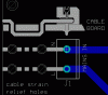
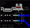
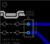
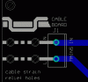
Attachments
Last edited:
")
")