Continue to Site

Welcome to our site!

Electro Tech is an online community (with over 170,000 members) who enjoy talking about and building electronic circuits, projects and gadgets. To participate you need to register. Registration is free. Click here to register now.

  • Welcome to our site! Electro Tech is an online community (with over 170,000 members) who enjoy talking about and building electronic circuits, projects and gadgets. To participate you need to register. Registration is free. Click here to register now.

How does this transistor ever turn on?

Status
Not open for further replies.

upand_at_them

Active Member
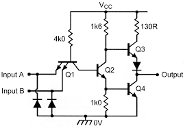
The image is a schematic of a 2-input NAND gate inside the SN7400. I'm confused how Q2 ever gets base current from the collector of Q1. My understanding is that when Q1 emitters are low, current flows from base to emitter...and since there's no voltage at the collector, no collector current flows. And when Q1 emitters are high, no base current flows...and there still is no collector current. I simulated this - with a one emitter NPN - on falstad.com and got the same results.

But clearly it must work. When Q1 emitters are high, Q2 base current must flow and turn on the transistor (which then turns off Q3 and turns on Q4). But how does Q2 get any base current?
download.png
 
Q1 (a&b) have a diode from Base to Collector that will pass current from Vcc----4k0 resistor----Q4 Base.
I know there is no arrow on the B-C of the transistor but there is a diode. It is not normally used if this manor.
 
It passes current whenever the B-C diode is forward biased? I can test this with any old NPN? I would have thought that would have worked in the falstad sim.
 
I would have thought that would have worked in the falstad sim.
That is a simple simulator which may not simulate all the characteristics of a real transistor.
I use free LTspice, which is a true Spice simulator that uses complex models.

Below is the LTspice sim of the input circuit.
I had to use two parallel transistors to emulate the dual-emitter transistor of the real circuit.

When either or both inputs are low, R3's current is flowing out Q2's and/or Q3's emitter to the input and no current goes to the base of Q1.
When both inputs are high, Q2/Q3 act as a transistor in the reverse direction with current from R3 and the input flowing to Q1's base.

This can be built with real transistors if you want to test an actual circuit.

1594308544133.png
 
Last edited:
If you replace the input transistors with diodes the circuit will function. (B-E diode & B-C diode)
 
Think of a single transistor and what happens when you place a resistor across the base and collector. In this sense, you essentially have two transistors in series with a total of 5.6k across two B-C junctions.

With the inputs floating, Q1,Q2 and Q4 are actually Saturated and fully "ON" , making the output LOW, keeping Q3 "OFF"

If any or both of the inputs are LOW, then Q1 is basically an "emitter follower" and will present the LOW signal to Q2 thus turning it and Q4 "OFF". At this time Q3 sees 1.73k across it's B-C junction and turns "ON", making the output HIGH.


BTW) here is a falsted sim ....

 
That circuit won't change states until both inputs are grounded, which you circuit doesn't show.
I think you mean that either input is grounded.

The inputs on TTL pull high if left unconnected. The input current is negative, meaning that current flows out of the inputs, especially when they are low.

The simulation shows the logic action if the switches are left closed, and the inputs are toggled between H and L.
 
That circuit won't change states until both inputs are grounded, which you circuit doesn't show.
Did you try it? The circuit simulation in post #5 is missing Q3 and Q4 where there is an inversion taking place ... So in a sense the simulation is depicting an AND gate not a NAND gate. From the perspective of the AND gate simulation you are not wrong except both inputs would be HIGH rather than grounded (LOW) in order to change state.

If any or both of the inputs re LOW, then Q1 is basically an "emitter follower" and will present the LOW signal to Q2 thus turning it and Q4 "OFF". At this time Q3 sees 1.73k across it's B-C junction and turns "ON", making the output HIGH.


It's a NAND gate ... doing exactly what it is intended to do ...
 
Last edited:
Here's a schematic of the Falstad simulation.
I see no connection to pull the inputs low, and a high input is the same as an open input in TTL.

(And yes, I was incorrect, only one input needs to go low for the output to change state.)

1594399440955.png
 
Status
Not open for further replies.

Latest threads

New Articles From Microcontroller Tips

Back
Top