Continue to Site

Welcome to our site!

Electro Tech is an online community (with over 170,000 members) who enjoy talking about and building electronic circuits, projects and gadgets. To participate you need to register. Registration is free. Click here to register now.

  • Welcome to our site! Electro Tech is an online community (with over 170,000 members) who enjoy talking about and building electronic circuits, projects and gadgets. To participate you need to register. Registration is free. Click here to register now.

Help needed on designing a circuit for a digital clock (A level project)

Status
Not open for further replies.
like this?
 

Attachments

  • time base-21..jpg
    time base-21..jpg
    61.2 KB · Views: 291
No.

Look at the datasheet for the ICs and note which pins go to the power supply.

Hint: the capacitor is short circuited how you've shown it.
 
I mean to connect the capacitor from one power rail to the other, from positive to 0V.
 
like this? just roughly.
But the reset of the first ic is connected to the ground pin, so wont the capacitor reset the ic?
 

Attachments

  • time base-24..jpg
    time base-24..jpg
    64.3 KB · Views: 292
That's it, you got there, in the end.

Now you can research why the capacitors are required, because if you're doing a course which is worth its salt, then it's the kind of question you'll be asked in the exam.
 
actually, i am doing a product design course, which doesn't involv any electronics, but i decided to do a project with electronics for extra credit. But ill research it so i have a better understanding :).
 
this is the minute circuit layout i made
is that what you mean by a capacitor across? only one?
and on the first ic, the circuit diagram that mbarazeen put up, the reset is attached to the 0V pin of the ic, wouldnt that reset the chip? or is that that the purpose?
could you reply asap please, its urgent.


edit*
ive just realised the first ic power pins are connected to the wrong rails
 

Attachments

  • minute circuit layout.JPG
    minute circuit layout.JPG
    55.1 KB · Views: 289
Last edited:
Each IC should have a capacitor across its supply rails.

The reset pin is activated by a logic high so no.

All unused inputs should be connected to either high or low.
 
here is the final circuit layout.
I have looked over it and all the connections are correct.
I am just asking if the connections i did with the unused pins to the ground rail are correct?
and if the circuit would work.
 

Attachments

  • untitled.JPG
    untitled.JPG
    49.1 KB · Views: 269
Yes, all unused inputs should go to 0V.

Don't connect an output to a supply rail because you could destry the IC.

You should be able to get rid of most of those ugly jumper wires by routing the PCB more carefully; connecting wires are not good and should be avoided wherever possible.

To ensure propper etching, it's good practise to chamfer all 90° corners.
 
Another jumper can be eliminated, possibly even more but I've not looked that hard.

Ideally the supply decoupling capacitors should be nearer the ICs, as close as possible.

As many corners should be removed as possible.
 

Attachments

  • A-level clock.PNG
    A-level clock.PNG
    12.7 KB · Views: 279
MutantNoodles,

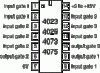
you need a small correction on the diagram i posted, its a mistake, to make divide by 12,000..the pin connections are wrong.
all should be shifted by one down on the diagram, ie:
the out puts 7,5,4,14,13,15 &2 has to be connected to AND gates. on the circuit it has been connected to 5,4,6,13,15,1,3 its wrong.
(Pin 3 is 15th bit out put and when it goes hight the ocunter resets. i confused this point before.)

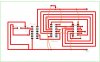
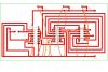
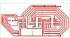
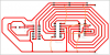
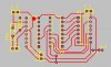
about PCB layout, you can rotate and shift ICs so get short paths to make a good look, also the out puts of 4060 can be connected to any of the inputs of AND gate, so change the connections to minimize jumpers. if possible i will post you an example how it can be.

Edit: see the PCB for an example with corrected circuit, you can follow your own style to improve your self.
 

Attachments

  • PCB1.JPG
    PCB1.JPG
    67.7 KB · Views: 300
Last edited:
for example, on the and gates, why are two of the 3rd input pins connected together?
please reply asap its urgent
 

Attachments

  • pins.gif
    pins.gif
    8.1 KB · Views: 271
the out puts 7,5,4,14,13,15 &2 has to be connected to AND gates. on the circuit it has been connected to 5,4,6,13,15,1,3 its wrong.
(Pin 3 is 15th bit out put and when it goes hight the ocunter resets. i confused this point before.)

When you say outputs do you mean pins, or outputs?
because when you say outputs 7 5 and 4, like you did in the diagram, thats the pins, and the outputs are Q4, Q5, Q6.
?
 
hopefully the circuit will work, the IC i selected for AND gate is 74HC11, see the datasheet, if you want to use 4073 then you have to make a minor change. on PCB rouite.
( swipe track to pin 8 & 9, connect 10 & 11, pin 14 of 4060 connect it to pin 12 of 4073)

for power supply, give the input across capacitor C1.
 
Status
Not open for further replies.

Latest threads

Back
Top