Continue to Site

Welcome to our site!

Electro Tech is an online community (with over 170,000 members) who enjoy talking about and building electronic circuits, projects and gadgets. To participate you need to register. Registration is free. Click here to register now.

  • Welcome to our site! Electro Tech is an online community (with over 170,000 members) who enjoy talking about and building electronic circuits, projects and gadgets. To participate you need to register. Registration is free. Click here to register now.

FPGA Hardware PCB

Status
Not open for further replies.

wuchy143

Member
Hi All,

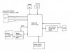
I"m working on my first real FPGA board and have a couple questions. Block level is attached.

1. How do you usually get all the pin assignments for the FPGA into a schematic capture tool? Is this really done manually?

2. Does anyone know where I can find information on how to connect up and FPGA for LVDS?

Regards,

-mike
 

Attachments

  • untitled.JPG
    untitled.JPG
    35.7 KB · Views: 340
The schematic capture symbol can be made and conneted manually like any other component. BUt yeah, it is a PITA to do with larger BGAs.

THere is software like FPGA System Planner can do it for you though to try and optimize routing based on a set of constraints (which signals can go to what types of pins). But it tends to only come with schematic capture software that costs money.
 
Last edited:
yeh. I figured the whole PITA thing would be unavoidable. :(

I have worked with the ISE/EDK/SDK quite a bit doing simple projects and what not. Really powerful tools. I've been able(using a dev board) to get microblaze up to do the "helloworld" as well. So, my next step is to do my own actual PCB with my FPGA on it which has microblaze in there running. If I can do that perhaps I will get hired on an FPGA team. At least that's my goal as that's where I will learn the most in the shortest amount of time.

Cheers to FPGAs

-mike
 
the likelihood of your being able to deal with a 600pin BGA is phenomenally miniscule. I design with FPGAs as part of my job and an ordered not touch one of those. You need to be able to be able to do at least a 6 layer PCB with buried vias and a grid of pads at 0.5mm or less pitch. You then need to place and solder the BGA when there is no way to get the heat to the pads to melt the solder with the only way to verify the soldering quality being an xray machine.

I can design the board, place and solder the BGA, but we can not justify the purchase of the xray nor desire the expense of sending all our boards out for the test.

You should concentrate on an FPGA that is NOT a BGA.

LVDS is a common interface that is readily available on FPGAs

**broken link removed** has LVDS and PLL and, and, and it is instant on flash.
 
You're talking about in-house mounting of the BGAs right? Because if you pay to have it mounted and x-rayed I don't see how there's a problem (of course, $$$). I've been wrestling with the idea of dishing out a bunch of cash to have a some FPGA processing modules made. It's expensive for the 8-layer board and BGA mounting but the bigger problem is the risk involved. I estimated it would come in at $800 a board rather than $600 which is what it cost to buy a module that doesn't have exactly what I want.

I recently found a module that costs only $300 though but it still doesn't have what I want (the big drawback to this board is the fixed frequency crystal for the FPGA rather than a configurable PLL). And the power supply is "just enough". It lacks a few startup measures that are good for FPGAs. But the cost is just too cheap for me to ignore!
 
Last edited:
dknguyen I believe you are correct. I have a friend who is an old dog with fpga's and that's exactly what he does for his boards. Though it would be cool to be able to do it all in house but I don't have that type of cash flow. :(
 
Yeah, i Know what you mean lol. The cost and risk is so high that even if there was no risk, you would need to make 3 or 4 to come within the cost range where it starts to become comparable with pre-bought solutions. That's not so much of a problem with me since I need at least that many anyways but...the risk!

At the least the FPGA processing modules are fairly tolerant to wiring mismatches as long as it doesn't involve the configuration, clocks, or power. I don't even care about the mounting costs really...not when compared to the 8-layer board. ARGH!!!!!
 
Last edited:
Don't use a BGA package. Instead, use a TPFQ package with a smller part, like the XC3S50A. You can just hand soldier it.
 
Status
Not open for further replies.

Latest threads

Back
Top