You can right click on the LM339 and pick another part. Something like it.I tried to import your drawing in LTspice but it cannot find the LM339
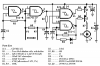
Many comparitors do not work well then their inputs are near VCC. Check the data sheet for input range. Most work from -0.4V to VCC-1.5V. So we might have to change things a little. At 80% duty cycle the input will probably be too high. Do you a supply other than +5V?