Continue to Site

Welcome to our site!

Electro Tech is an online community (with over 170,000 members) who enjoy talking about and building electronic circuits, projects and gadgets. To participate you need to register. Registration is free. Click here to register now.

  • Welcome to our site! Electro Tech is an online community (with over 170,000 members) who enjoy talking about and building electronic circuits, projects and gadgets. To participate you need to register. Registration is free. Click here to register now.

Design Help --- Bubba Oscillator

Status
Not open for further replies.
i was looking at the data sheet of the cd4047 and it looks like quite a task to construct such a diagram. do you by any chance have somehind i can use other than or do you already have a constructed one.
 
Hi audioguru, thanks for your suggestion. You are correct i we use straightly use the sine wave bubba oscillator to drive the mosfets or igbt means it will be like an heater. and also we need the huge transformers.

If i am not wrong, that they are two approches for designing the inverters

1. Convert the low voltage DC to high voltage DC, then make this HV DC in to HV sine wave AC.

2. Using the high power mosfets or igbt that will oscillate at 50 hz in the primary of the larger transormer to produce the 230V.

I think the first approach the best and efficient. Because there is no need of large transformers and also we using the PWM techniques which is more efficient.

So my approach is the first one.

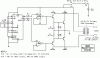
The overall project splitted into two main blocks

1. DC -> DC converter
2. DC -> AC converter

1. DC -> DC converter blocks
a. PWM control
b. Half bridge driver

2. DC -> AC converter blocks
a. Sinusoidal PWM control
b. Full-bridge driver
c. Low pass filter

So welcome all of your suggestions for implementation, design and analysis of the above said blocks.
 
So first we need to design is the PWM control for the DC->DC converter.

Points to consider is the
1. How to generate the PWM signal. By using the uC or the PWM chips.
2. What is the frequency of the PWM signal.
3. How to design feedback control to vary the duty cycle or the frequency of the PWM.
4. What is the duty cycle of the PWM.
 
without cutting you short prabhueng but let me ask you a question. i got the circuit that you designed online with the monostable vibrator the cd4047. what is it used for the the circuit, is it just the switch the voltages on and off at a desired frequency?
 
i got the circuit that you designed online with the monostable vibrator the cd4047. what is it used for the the circuit, is it just the switch the voltages on and off at a desired frequency?
We don't see the circuit.
The CD4047 is usually used as the oscillator in a square-wave inverter since it has two opposing perfect square-wave outputs. Its mono-stable function is not used. The opposing outputs drive push-pull power transistors or Mosfets that drive a center-tapped transformer.

A TL494 or other PWM IC is used for a sine-wave inverter.
 
Yes we can use the TL494 for the PWM generation.
One more thing can I use SG3525 for PWM generation.

I need to check first whether these two IC's are available in my place.
If not available I planned to use the ATmega8 uC for PWM generation.

The inverters power output is 300W. So the input is 12V and 25 Amps. Please tell me which MOSFET can handle this much current. Or can I use bank of MOSFETS for this much current.

Whether single MOSFET or bank of MOSFET which is better?

What is the deadtime concept in handling the MOSFET?
 
Almost any low voltage Mosfet will pass 25A. Some have a very low on-resistance so they will not have much loss and will not get too hot.

Maybe use 50A or more Mosfets so that they will survive if the inverter is overloaded. Then a circuit breaker will have enough time to blow.

Deadtime allows one side to turn off before the other side turns on to avoid an extremely high current from the supply voltage to ground.
 
Hi audioguru

I got both TL494 & SG3525 chips for Rs24.

Also I choosed to use IRFZ48 MOSFET for the DC-DC conversion step.

Now I reading the TL494 examples to construct the DC->DC conversion circuit design.

After constructing the circuit I will post it.

Now my major confusion is selecting the transformer?
Please share me any idea for the transormer selection.

Specification is

primary
-----------
V=12
A=30

Secondary
----------------
V=350
A=2

Because I am using the PWM with high frequency means I can use the Ferrite core. But what is the standard or the size of the Ferrite core?....
 
I have never used and never made an inverter so I cannot help your design.
 
i have a question once more..... for the astable vibrator in the attached diagram, what formula is used to calculate the frequency with which it switches the signals.
 

Attachments

  • 200715103930_100W inverter (1).GIF
    200715103930_100W inverter (1).GIF
    14.9 KB · Views: 909
i have a question once more..... for the astable vibrator in the attached diagram, what formula is used to calculate the frequency with which it switches the signals.
You simply look at the datasheet for the CD4047 and it tells you everything about it.

The datasheet from Texas Instruments has more details than from other manufacturers. It has the formula and many graphs showing accuracy when the temperature, supply voltage, frequency, capacitor value and resistance is changed.

Note that the oscillator runs at double the output frequency because it hase a frequency divider so that its outputs have exactly 50:50 duty-cycle.
 
a quick qestion guys, i built the inverter circuit in its entirety i think. but when i powered it on i realise that the power supply 12 dropped to 0 which i think is more or less a failsafe if there is a problem. i rechecked the wiring and everything seems fine. i my say that i used a 24 volt secondary center tapped and i noticed that the a stable vibrators oscout is not connected to anything. is it supposed to be that was? any suggestions as to why the circuit does not give any output on the oscilloscope?
 
a quick qestion guys, i built the inverter circuit in its entirety i think. but when i powered it on i realise that the power supply 12 dropped to 0 which i think is more or less a failsafe if there is a problem.
There is no power supply. The 12V comes from a powerful lead-acid battery. If the 12V drops to 0V then your battery is not charged or the 15A fuse is blown.

I noticed that the astable vibrator's oscout is not connected to anything. Is it supposed to be that was?
The OSCOUT is not used. The Q and Q-not outputs are at the mains frequency.

any suggestions as to why the circuit does not give any output on the oscilloscope?
The Q and Q-not outputs of the CD4047 should show a square-wave at the mains frequency with an amplitude of 13V.
The outputs of the opamps should show a square-wave at the mains frequency with an amplitude of about 1.2V to 2.2V.

The collectors of the output transistors should show a square-wave at the mains frequency with an amplitude of about 22V.
 
Last edited:
I am actually not using a battery. i am actually testing it using a power supply. let me post you a setup in a minute
 
this is the setup as you can see there is not battery connected just a power supply.
 

Attachments

  • 1104091500a.jpg
    1104091500a.jpg
    389.4 KB · Views: 633
  • 1104091500b.jpg
    1104091500b.jpg
    401.2 KB · Views: 697
You cannot make an inverter on a breadboard!
The contacts are ruined where you forced the huge pins on the 2N3055 transistors into them.
Them and the other connections cannot conduct 15A and neither can your thin wires.

I doubt that your power supply can supply 15A.

There is no heatsink on the power transistors and driver transistors!
 
ok now i am setting it up piece by piece. i get vp of 13 volts on the q and qnot outputs. i think the problem might be in the amplifier circuit.
 
There is no amplifier. Just a pair of driver transistors and a pair of output transistors.
They simply switch on and off, they do not amplify.
 
Status
Not open for further replies.

Latest threads

New Articles From Microcontroller Tips

Back
Top