Continue to Site

Welcome to our site!

Electro Tech is an online community (with over 170,000 members) who enjoy talking about and building electronic circuits, projects and gadgets. To participate you need to register. Registration is free. Click here to register now.

  • Welcome to our site! Electro Tech is an online community (with over 170,000 members) who enjoy talking about and building electronic circuits, projects and gadgets. To participate you need to register. Registration is free. Click here to register now.

decoupling capacitors

Status
Not open for further replies.

electricity86

New Member
In many designs i saw that the same capacitors, for example number of 0.1uF capacitors in parallel to 2.2uF capcitor, are all connected in parallel to an input pin.

What is the advantage of it over using only one 0.1uF with one 2.2uF?

Does the first method increases the frequency range where the total impedance is low?
 
0.1µF capacitors have better high frequency charicteristics than 2.2µF capacitors.
 
For effective bypassing at very high frequencies the caps have to be very close to the components they are to bypass (or de-glitch).
 
The 2.2µF capacitor is better at lower frequencies.

Putting both together gives capacitor that's both good at filtering low as well as high frequencies.
 
Thank you for your answers.

I'm not asking why to put single 2.2uF with single 0.1uF.
I'm asking why to put single 2.2uF with five 0.1uF? (five, four, any number thats larger than one).
 
Seems overkill to me electricity. Some circuits I've seen do use more than one value of bypass cap but I wouldn't bother unless you end up having noise problems with the .1u ones.
 
.1u is good for high frequencies. 2.2u is good for low frequencies. Both together is for both high and low frequencies.
Understand now?
 
You'll also often see 1:mu: + 100n + 1n connected in parallel for exactly the same reason.
 
Connecting ceramic capacitors in parallel is generally bad practice. Generally (again), the best bypassing is done by having a large bulk electrolytic (or tantalum), something with some amount of ESR to it say 100mOhm or 200mOhm and then a single ceramic cap at the package, with the ceramic cap being the largest value that's cost-effective in its case size.

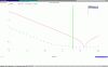
Frequently I'll read that .1uF caps are better at bypassing HF than say a 1uF or larger. ESL is actually determined mostly by the case size (0805, 0603, whatever) and less dependent on the value (though it is to some degree). Attached are impedance plots for a .1uF, 1uF, and 2.2uF all 10V 0805 size capacitors from Kemet. Note how the high frequency performance converges.

Putting a 2.2uF ceramic and a .1uF ceramic on parallel is bad practice, even though you'll see app notes that tell you to do it. Same with 100nF and 1nF. You end up with good bypassing near the resonant impedance nulls of each capacitor, but in between you can and will usually get a nice LC resonance due to parasitic inductance. I had coworkers that refused to believe me on this point til one of the company's PhD's over in design backed me up on it. There's papers out there on the net with graphs if you care to go looking.
 

Attachments

  • untitled.GIF
    untitled.GIF
    28.1 KB · Views: 136
To demonstrate further, here is a plot of two 100nF capacitors. One is 0805 and the other is 0402. Notice how superior the 0402 is due to lower ESR/ESL. The 0805 has almost twice the ESL (1.94nH vs. 1.04nH).
 

Attachments

  • untitled.GIF
    untitled.GIF
    24.5 KB · Views: 139
Last edited:
I assumed the 2.2:mu:F capacitor was electrolytic.

You've raised another valid point though, SMT parts are better than through hole because they have a lower inductance.
 
But why to use from the beginning a number of 0.1uF?

There is no point putting several capacitors in parallel if they are in the same place.

However, they won't be close together. The 0.1 µF capacitors will be spread around the circuit board, as flat5 said. Speakerguy79 pointed out that 0402 capacitors have 0.9 nH less inductance than 0805 capacitors, but failed to point out that the difference is equivalent to just 1mm of PCB track.

Analog Devices: Analog Dialogue: Ask The Applications Engineer - 10

So to get the ESL down, it is no good to just use good capacitors, you have to put them close to where the noise comes from, normally the power pins of the ICs. Some ICs have several power pins spread around the IC so that the effect of the lead inductance can be reduced if each power pin has its own capacitor to ground.

This is where circuit diagrams don't show the whole picture. If high frequencies are present, track inductance is important and it depends on track length. The circuit diagram does not show the layout, so does not show what the track inductance might be.

I have seen circuit diagrams where there is a capacitor shown near each IC, as there is in the layout. I have also seen circuit diagrams where the decoupling capacitors are shown all in parallel off to one side so that the lines don't cross the logic lines, so as to make the logic easier to follow. Both are correct, but neither shows the layout.
 
All caps are not created equal Diver, using differing types of caps in parallel even right next to each other can improve noise reduction.
 
Yes, you are quite right.

I meant to say several identical capacitors, and I should have qualified it further as I was referring to the 0.1 µF capacitors that the OP was asking about.

Also, in the case of larger capacitors, increasing the capacitance or decreasing the ESR can be achieved by paralleling several.

My main point was the importance of distributing the capacitance around the circuit board.
 
Thanks guys.
I picked up alot of information in this thread and wanted to verify some things in your permission.

a. Why SMD components have lower inductance then through-hole components, and why small-case size sMDs have lower inductance than large-case ones?
You got maybe an article regarding that?

b.
Diver300
"So to get the ESL down, it is no good to just use good capacitors, you have to put them close to where the noise comes from, normally the power pins of the ICs|

Why are power pins of ICs are being source to AC noise?

c.
Do you recommend transferring all through-hole electrolytes to SMD ones? to decrease ESL?

Thanks a lot.
 
When the transistors inside and IC switch, there is a current spike. This either comes from the charging or discharging capacitances or when both the pull-up and pull-down transistors are both on at the same time for a few nanoseconds.

This current is in one or both power lines and it starts and stops very quickly, so any inductance in the power lines will make the voltage on the power lines bounce. Ground bounce - Wikipedia, the free encyclopedia

Placing the capacitors close to the ICs minimises the distance that the current spike has to travel. That minimises the loop inductance, and therefore the level of the ground bounce.
 
Thanks.

So how do you prevent this spikes from happening when the power goes from high to low or from low to high?
The large electrolyte capacitor should now provide the current spike to the IC?
 
Status
Not open for further replies.

Latest threads

New Articles From Microcontroller Tips

Back
Top