Continue to Site

Welcome to our site!

Electro Tech is an online community (with over 170,000 members) who enjoy talking about and building electronic circuits, projects and gadgets. To participate you need to register. Registration is free. Click here to register now.

  • Welcome to our site! Electro Tech is an online community (with over 170,000 members) who enjoy talking about and building electronic circuits, projects and gadgets. To participate you need to register. Registration is free. Click here to register now.

Change Pot in Mini Buck Converter

Status
Not open for further replies.
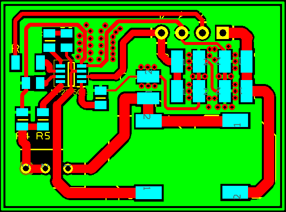
Continuous copper pour.
BUCK PCB Pour.png
 
CDRH104RNP-221NC
CDRH104RT125NP-4R7PC

Its an Ebay seller. I know you guys dont like buying components from here but if you dont care for these i can keep looking
Thanks for the datasheets. As for buying parts from ebay, that's OK as long as you get what you expect. Ebay sellers often don't give you the the part number or data to let you find out the parasitic specs of the part.

The part you've chosen for L1 is good. The two current rating are a comfortable margin above your operating current.

But L2 is going to be a problem. It's saturation current is only 0.95 Amps. So at 3 amps it's lost it's inductive properties, and will just be a wire with 560 milliOhms of resistance. Which, at 3 amps, will dissipate about 5 Watts of heat.

As Diver300 said in post # 41, ceramic capacitors suffer from reduced capacity that varies with operating voltage. I don't know what parts you are using, but here is a link to the characteristics chart of one possible part.
https://media.digikey.com/pdf/Data Sheets/Samsung PDFs/CL21A226MAYNNN_CharSheet.pdf
The graph to look at is the DC Bias Characteristics. Notice that at 12 Volts, the part has lost over 80% of it's capacitance. So what should be 22uF, is really less than 5uF. Now, ceramic capacitors can still be used, but you need to chose the parts wisely and compensate for as needed.

Electrolytic caps don't have this issue.
 
But L2 is going to be a problem. It's saturation current is only 0.95 Amps. So at 3 amps it's lost it's inductive properties, and will just be a wire with 560 milliOhms of resistance. Which, at 3 amps, will dissipate about 5 Watts of heat.
Here is a passage from the author and his use of L2.

"C1 and C2 are used to reduce input voltage noises. R2, R4, and R5 build a feedback path to the chip. R2 is a 200K multiturn potentiometer to adjust the output voltage. L1 and C4 are the essential buck converter elements. L2, C5, and C7 make an additional output LC filter that I added to reduce the noise and ripple. The cut-off frequency of this filter is around 1KHz. R6 limits the current flow to the EN pin."

If that means the inductor is ok for its intended purpose in this circuit thats good. If not ill find another substitute for the 4.7uh inductor.
 
The graph to look at is the DC Bias Characteristics. Notice that at 12 Volts, the part has lost over 80% of it's capacitance. So what should be 22uF, is really less than 5uF. Now, ceramic capacitors can still be used, but you need to chose the parts wisely and compensate for as needed.
If the CDRH104RT125NP-4R7PC is not suitable for the application described above i have located CDRH3D16/HPNP-4R7NC. And while i do appreciate your sharing with me what value is important I do not know what im looking at. The original 4.7uh part says 5.57 under saturation current and this new one says 1.20 so I dont know how .95 was calculated. If you could look at this Inductor and tell me what you think.
 
Last edited:
No Im the one who is incorrect. I probably need a vacation.
So the main point is the same i just confused the 4.7uf with the 221uf part. The role of L2 is to act as a noise filter. He states it as an LC filter. So is L2 (220uh) suitable because of how it is implemented in the circuit or do I need one with a higher SI?
 
Last edited:
I went back to the parts list supplied by the author. He does list L1,2 as having 3A. I however, cannot locate a 220uh with that high of a rating. I used Digi-Keys Search Tool and found just 1 with a 3A rating. I sent a message to the author asking to clarify his part numbers.

This is L2 on his board. No way thats rated @ 3Amp. Its so small.
1647055990483.png

This is L1 4.7uh. Opposite side
1647056201665.png
 
Last edited:
I believe i found the part numbers.
DR1050-4R7-R (L1)
DR1050-221-R (L2)
-------------------------------------------
It appears that the components I had located on Ebay are very close in their Amp ratings. My 220uh is rated slightly higher but the 4.7uh I selected is rated at 5.57A and the Eaton component is 6.2a
1647057122355.png
1647057984629.png
 
One reason that higher inductances have higher resistance and lower current capacity, is that it takes more turns of wire to get the higher inductance. If the body size is the same, it means you have a longer piece of a thinner wire.

But, you really don't need that much inductance for the noise filter. The author said that the cutoff frequency of the filter is about 1KHz, which is correct for those values. But the switching frequency for the mp2315 is 500khZ. There is no reason to set the cutoff so low. In this case, I would use the same 4.7uF inductor for L2 as L1. That inductance, with the existing capacitance, has a cutoff frequency of about 15KHz. Still well below the switching frequency.

What is the highest voltage you want the output to go to? The 200 K pot will let you go to about 24 volts. But you'll need about 27 Volts on the input to do so.
 
What is the highest voltage you want the output to go to? The 200 K pot will let you go to about 24 volts. But you'll need about 27 Volts on the input to do so.
So glad you asked. I was trying to explain to my wife that I would never go above 12 volts output but she just gave me a strange glare. So yes. This as designed is capable of 24V input I would apply a max of 15V. And the output range would be 12V to 3.3V. From what i understand the greater the range of input / output (24v in / 5v out) the hotter the inductor gets.
But, you really don't need that much inductance for the noise filter. The author said that the cutoff frequency of the filter is about 1KHz, which is correct for those values. But the switching frequency for the mp2315 is 500khZ. There is no reason to set the cutoff so low. In this case, I would use the same 4.7uF inductor for L2 as L1. That inductance, with the existing capacitance, has a cutoff frequency of about 15KHz. Still well below the switching frequency.
Great! that makes it a bit easier for me to purchase. Thank you. So if im using 4.7uh for L1 L2 it would have no effect on the input/output voltage ranges as L2 is just being used as a noise filter.
 
The author responded with this message
"Yes you can use another 4.7uH and use a bigger capacitor near your load as I did in the video. its job is just filtering."
He also suggested a big fat 470uf cap across the input for additional noise filtering.
 
Ive updated the design with mounting posts and replaced the via shielding array with a few placed vias that are meant to evenly connect the top copper GND layer with the bottom GND layer. That is how i understand its purpose. Ive increased the tracks as wide as possible with the exception of the GND track as the pour will widen them. I am extremely grateful for everyone in this group. Learned so much about so many new features and components.

BUCK PCB3 with vias2f.png
 
An alternative to wide tracks is multiple pours bound to nets
Ive highlighted each net in a different color. Shown encapsulating their associated tracks in red.
It does not encapsulate every track but my point is you can do this instead of beefy tracks. Of course where it cannot be done due to constraints the tracks close to the IC have beefed up tracks.

The ground pour is in green and it is continuous. It reaches every pad where ground is needed. The through hole header pin (in green with arrow) is linked to the bottom layer which joins them together. I added 4 ground vias (circled) that are intended to make a better (more even) connection with the bottom ground plane.

The four corner mounting holes are not linked to anything (isolated) so i dont know if these serve or can serve any additional purpose other than to mount the board. If connecting these to a net or ground will improve anything please let me know.

My understanding of pours, tracks, and overall balance is still very weak. I rely heavily on your opinions to help me understand this.
Thank you.

BUCK PCB Pour2.png
 
An alternative to wide tracks is multiple pours bound to nets
Ive highlighted each net in a different color. Shown encapsulating their associated tracks in red.
It does not encapsulate every track but my point is you can do this instead of beefy tracks. Of course where it cannot be done due to constraints the tracks close to the IC have beefed up tracks.

The ground pour is in green and it is continuous. It reaches every pad where ground is needed. The through hole header pin (in green with arrow) is linked to the bottom layer which joins them together. I added 4 ground vias (circled) that are intended to make a better (more even) connection with the bottom ground plane.

The four corner mounting holes are not linked to anything (isolated) so i dont know if these serve or can serve any additional purpose other than to mount the board. If connecting these to a net or ground will improve anything please let me know.

My understanding of pours, tracks, and overall balance is still very weak. I rely heavily on your opinions to help me understand this.
Thank you.

View attachment 136210

I like this approach better than the previous layouts.
However, I'm not clear on the colors other than green. What is the relationship between the wide red trace and the purple pour, for example?

Don't forget to widen the thermal spokes.
 
However, I'm not clear on the colors other than green. What is the relationship between the wide red trace and the purple pour, for example?
It is just so you can see the red track and the pour at the same time. Perhaps if I did this it would be better understood. Now this shows that after production the tracks will be one with the pour. Yes the spokes are 2.5 times larger this shows 10 in size. the new spoke width is 25.


BUCK PCB Pour2.png

BTW. does this image remind you of anything?

Partiridge Family.png
 
On that buck converter, the current in the supply (pin 2), ground (pin 4) and the capacitors between those pins are where the varying current flow.
It's a good idea to keep that path as short as possible. I suggest you move the capacitors closer to the IC, or put a small ceramic capacitor very close to the IC between pins 2 and 4.
OK. So if possible move C2 closer or add an additional cap
BUCK PCB Cap Move.png
 
It is just so you can see the red track and the pour at the same time. Perhaps if I did this it would be better understood. Now this shows that after production the tracks will be one with the pour. Yes the spokes are 2.5 times larger this shows 10 in size. the new spoke width is 25.
Ok...the image is confusing to me but whatever works for you is ok.

BTW. does this image remind you of anything?

Heh....yeah....the 70's....:hilarious::joyful:
:joyful:
 
Ok...the image is confusing to me but whatever works for you is ok.
Ok this is unfilled. Only the outlines of the separate net pours.
The White arrows point to the perimeter of each pour. Ive carefuly drawn the pours (all on top layer) so they produce spokes and done take away from other pour areas. Many are just a fraction from each other. You can see the pour goes around a pad on C4. And another odd shaped pour area goes around a pad on C3. All designed to put spokes around the pad. If any of these pours are in error or could be improved just let me know.

BUCK PCB Pour3.png


With pour. Here it is shown with all but the ground pour. Thats how my software does it.
BUCK PCB Pour3a.png
 
Status
Not open for further replies.

Latest threads

New Articles From Microcontroller Tips

Back
Top