Continue to Site

Welcome to our site!

Electro Tech is an online community (with over 170,000 members) who enjoy talking about and building electronic circuits, projects and gadgets. To participate you need to register. Registration is free. Click here to register now.

  • Welcome to our site! Electro Tech is an online community (with over 170,000 members) who enjoy talking about and building electronic circuits, projects and gadgets. To participate you need to register. Registration is free. Click here to register now.

Camera FPGA PSRAM interface check

Status
Not open for further replies.

freeskier89

New Member
Hey there,

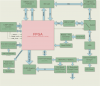
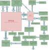
I am designing a handheld device and I was hoping that I could get some comments/critiques on the structure of it from those of you who are more experienced than I am (Which is probably everyone because I am 16 lol). I do not really want to disclose exactly what I will be making, but I think I will be able to give you enough info that you can see how it will be organized.

Here are the major things that will be performed:

1. Every once in a while the FPGA will "take a picture", which consists of receiving all of the image data from the camera and dumping it directly to the psram. When that is done, an edge detection algo will be run on the image, and other relatively easy byte by byte processing will occur.

2. The FPGA will display a simple color gui on a graphic lcd. (Most likely I will just take a different bitmap from ram an put it on the lcd and then just write text and a scroll bar on top of it)

3. When plugged into the computer, the device will either show up as a mass storage device or as serial port for my application to do stuff with it. I am not quite sure what I am going to do with this usb feature, but I want to have it because I know there will be a use for it later.

Do you think I will be overstressing the FPGA too much?

I attached a diagram I made that will hopefully clarify things a bit. I know there are still a lot of unknowns (like clock speed, etc...) but I kind of thought I would try to keep the initial description to a minimum :). Let me know what questions you have ;)

Thanks!

ps: I am not quite sure on the density of ram I am going to use, but I am thinking 4-16megabytes or PSRAM(aka cellularram)from Micron.
 

Attachments

  • Circuitry.png
    Circuitry.png
    76.4 KB · Views: 360
Sidestepping the whole "would probably be easier to do this on a PDA" issue -

The last time I stuck a x16 SRAM on a 144 pin FPGA, it ended up using up a very large chunk of the IO lines - 16 data + 21address + 4-5 control lines, that by itself is ~50% of the IO.

The PSRAM parts are BGA only which is an interesting exercise in solder reflow.

SRAM based FPGAs have very large quiescent currents. They'll eat up ~100mW or so just sitting there.

UI's are much, much easier to do in a large, well-padded microcontroller. You'll need a decent amount of space to store any text/graphics.

James
 
Yeah it would be a lot easier to do on a PDA, but for what I am doing, it would look a lot better if I designed the thing from scratch, and not to mention, I learn a lot more by designing it :).

About the SRAM/ I/O issue, I am going to be extremely tight on I/O. I have 65 to work with, and at the moment it looks like I will be using 65 :S. Potentially, I could hook up the data or address lines to a PISO Shift Register, but I that would make things more complicated, and would decrease performance considerably. Any thoughts? At the moment it looks like I will be fine on I/O, but as I come closer to actually drawing the schematics I am sure I will need more :(.I might have to hook up my status leds and such to the I2C bus lol, wouldnt that be fun. Here is the breakdown for what is using the I/O at the moment:

11-Camera
42-RAM
1-Low Battery Alarm
4-SPI Bus(LCD,ADC)
2-I2C Bus (Camera,Fuel Gauge)
3-SD
2-USB

I too was concerned about the BGA soldering. Luckily with a bit of research, it looks like it isn't too daunting of a task using a hot plate and a professionally made pcb. I doubt it will be painless though. I think soldering the iCSP44 package for the camera will be a bit more difficult yet because I believe they have much tighter temperature tolerances.

About the quiescent current, I had not thought of that before. Thanks for making me aware of that. I suppose I should plan on a larger battery. Would implementing a "sleeping" system with a MCU be a good workaround? After a minute or so of no usage, it could send a signal to a MCU to cut off its power and then restart it when the user shows interest again. The FPGA would have to reboot from the PROM each time though.

I was planning on loading the font for the graphic LCD from the SD card to the RAM upon start up. The FPGA could then grab each character from the RAM when it needs it. I will probably use a simple, non-antialiased, 5x7 bit font to keep it simple. The graphics will be stored and used similarly.

The whole GUI is going to be very minimalistic and will be nowhere near the complexity of a cell phone. Pretty much it will probably incorporate a startup screen, and a page showing the preview from the camera(not mandatory), along with a few dynamic textfields. Thats about it.

I would like to stay away from a MCU other than a PIC if at all possible, mainly because I do not really want to spend more money on a new programmer and the like. What exactly makes UIs easier to do on MCUs?

Thanks again for your response; it helps considerably :)
 
Last edited:
freeskier89 said:
Yeah it would be a lot easier to do on a PDA, but for what I am doing, it would look a lot better if I designed the thing from scratch, and not to mention, I learn a lot more by designing it :).
Fair enough.

freeskier89 said:
About the SRAM/ I/O issue, I am going to be extremely tight on I/O. I have 65 to work with, and at the moment it looks like I will be using 65 :S. Potentially, I could hook up the data or address lines to a PISO Shift Register, but I that would make things more complicated, and would decrease performance considerably. Any thoughts? At the moment it looks like I will be fine on I/O, but as I come closer to actually drawing the schematics I am sure I will need more :(.I might have to hook up my status leds and such to the I2C bus lol, wouldnt that be fun. Here is the breakdown for what is using the I/O at the moment:

Well, I'd recommend that you switch to a 8 bit bus for the PSRAM - unless you really think you need the bandwidth. Or add some address latches on the high order memory bits(i.e. the ones you don't need to change often). Alternatively use a DRAM chip and just deal with the added memory controller complexity, but with only half the address lines.

freeskier89 said:
I too was concerned about the BGA soldering. Luckily with a bit of research, it looks like it isn't too daunting of a task using a hot plate and a professionally made pcb. I doubt it will be painless though. I think soldering the iCSP44 package for the camera will be a bit more difficult yet because I believe they have much tighter temperature tolerances.
Well, there are CMOS sensors which have LCC style edge pinouts instead of BGA's. Those are easier to solder by hand.

freeskier89 said:
I was planning on loading the font for the graphic LCD from the SD card to the RAM upon start up. The FPGA could then grab each character from the RAM when it needs it. I will probably use a simple, non-antialiased, 5x7 bit font to keep it simple. The graphics will be stored and used similarly.

The whole GUI is going to be very minimalistic and will be nowhere near the complexity of a cell phone. Pretty much it will probably incorporate a startup screen, and a page showing the preview from the camera(not mandatory), along with a few dynamic textfields. Thats about it.

I would like to stay away from a MCU other than a PIC if at all possible, mainly because I do not really want to spend more money on a new programmer and the like. What exactly makes UIs easier to do on MCUs?

Well, having a font 'bootloader' makes things that much more complex, plus trying to hit the RAM (which might be in the middle of an image operation) to update the display means having a pretty complex state machine setup along with the required addressing/oddball multipart DMA setup... Have you tried coding the HDL that would do this yet, because it'll be an insane PITA. (BTW, it would probably be a better idea to hardcode the font into the FPGA's SRAM blocks, but it would still be pretty painful, and I can imagine the logic to do this taking a good 30% of the FPGA to implement).

Generally one has a uC in the system to handle all the stuff that happens at "user" speed - UI controls (getting a FPGA which is running at MHz speeds to deal with sub Hz user interactions means a lot of large delays/counters), display updates (having 10's of lines of C code or 100's of lines of assembly is much less painful than trying to debug a FPGA). As well as things that a FPGA is just bad at - "allocating" space in the SRAM for image buffers, initialization command sequences for the flash/sensor, or just doing more complex actions - storing multiple images in multiple buffers at different resolutions at different times, clipping subregions, formatting the images on the SD card with the correct image headers, etc.

James
 
hjames said:
Well, I'd recommend that you switch to a 8 bit bus for the PSRAM - unless you really think you need the bandwidth. Or add some address latches on the high order memory bits(i.e. the ones you don't need to change often). Alternatively use a DRAM chip and just deal with the added memory controller complexity, but with only half the address lines.
Initially I was thinking of using PSRAM with an 8 bit bus, but I switched to the 16 bit bus after I never found ram with the smaller bus. I will have to look into that a bit more.
hjames said:
Well, there are CMOS sensors which have LCC style edge pinouts instead of BGA's. Those are easier to solder by hand.
The only 1.3MP SoC camera I could find with the LCC package was the OV9620. I have looked extensively on the net to find a place I can buy them to no avail. No one want's to sell them to a student :(. I think the iCSP44 package will be alright, again the hot plate "should" be alright.
hjames said:
Well, having a font 'bootloader' makes things that much more complex, plus trying to hit the RAM (which might be in the middle of an image operation) to update the display means having a pretty complex state machine setup along with the required addressing/oddball multipart DMA setup... Have you tried coding the HDL that would do this yet, because it'll be an insane PITA. (BTW, it would probably be a better idea to hardcode the font into the FPGA's SRAM blocks, but it would still be pretty painful, and I can imagine the logic to do this taking a good 30% of the FPGA to implement).

Generally one has a uC in the system to handle all the stuff that happens at "user" speed - UI controls (getting a FPGA which is running at MHz speeds to deal with sub Hz user interactions means a lot of large delays/counters), display updates (having 10's of lines of C code or 100's of lines of assembly is much less painful than trying to debug a FPGA). As well as things that a FPGA is just bad at - "allocating" space in the SRAM for image buffers, initialization command sequences for the flash/sensor, or just doing more complex actions - storing multiple images in multiple buffers at different resolutions at different times, clipping subregions, formatting the images on the SD card with the correct image headers, etc.
Hmm... So do you suppose I should use the fpga for the main image processing and not much else? Then I could use a powerful MCU to display info on the LCD and control the basic user interface. I do not believe PICs are quite powerful enough, no? Maybe some of the 18 series ones would work. What do you think?
 
freeskier89 said:
Initially I was thinking of using PSRAM with an 8 bit bus, but I switched to the 16 bit bus after I never found ram with the smaller bus. I will have to look into that a bit more.
Well, that's easy- just don't connect them! (other than having some pull-ups of course). Alternatively, there's nothing wrong with having a non-standard bus width.

freeskier89 said:
The only 1.3MP SoC camera I could find with the LCC package was the OV9620. I have looked extensively on the net to find a place I can buy them to no avail. No one want's to sell them to a student :(. I think the iCSP44 package will be alright, again the hot plate "should" be alright. Hmm... So do you suppose I should use the fpga for the main image processing and not much else? Then I could use a powerful MCU to display info on the LCD and control the basic user interface. I do not believe PICs are quite powerful enough, no? Maybe some of the 18 series ones would work. What do you think?
Digikey seems to have a couple MT9T001P12STC's in stock. (3Mpixel, LCC packaging). Mouser used to carry some of www.st.com 's image sensors, but they seem to have stopped. (Surprise, cell phone parts don't stand still...)

An external PIC would be the safer approach - FPGA resources are pretty limited, and using them to do UI can definitely be a misuse of resources. I think nearly any uC with at least a Kbyte of ram would be more than enough - a 5x8 character map needs ~.5KBytes of ROM space at most, and that can be trimmed down pretty easily. Bigger chunks of data(images/backgrounds) can be retrieved from the EEPROM, or maybe even the FPGA's configuration flash via the FPGA.
 
hjames said:
Well, that's easy- just don't connect them! (other than having some pull-ups of course). Alternatively, there's nothing wrong with having a non-standard bus width.
I read you loud and clear now :D. So if I wanted 16MB of ram I would get a 32MB chip and then use all of its addresses, but just use half of the memory at each address. I do not know why I never thought of that lol. Or I suppose I could use one I/O pin from the fpga to go to a bus switch that would switch between the lower address bits and upper bits, but I do not think I will need to.

hjames said:
Digikey seems to have a couple MT9T001P12STC's in stock. (3Mpixel, LCC packaging). Mouser used to carry some of www.st.com 's image sensors, but they seem to have stopped. (Surprise, cell phone parts don't stand still...)
I checked out the MT0T001s but ruled them out mainly because it isn't a System on a Chip (SoC) sensor. I could do brightness/contrast/level adjustments on the FPGA, but I don't want to. I will be doing enough on it as it is :). At very first, I really wanted to use a VS6624 from ST because they have an integrated lens and flexstrip, but the quest for getting one went downhill because they aren't in production yet and only cell phone companies can get them. The MT9T111 will be a rather stressful item to solder, but other than that, I think it will be a perfect camera. I am the one that got Digikey to say they are not "Non-Stock" anymore :). One way or another Ill get it on the board even if I have to send it in.
hjames said:
An external PIC would be the safer approach - FPGA resources are pretty limited, and using them to do UI can definitely be a misuse of resources. I think nearly any uC with at least a Kbyte of ram would be more than enough - a 5x8 character map needs ~.5KBytes of ROM space at most, and that can be trimmed down pretty easily. Bigger chunks of data(images/backgrounds) can be retrieved from the EEPROM, or maybe even the FPGA's configuration flash via the FPGA.
Alright thanks. I will definitely look into which PIC will be best for my needs. For storing the images/backgrounds, I was going to store this on the SD card. I know, I know, it sounds a lot like overkill. The reason is that it could be easily plugged into the computer to modify, and I could easily has it enumerate as a USB mass storage drive using a USB2229 from SMSC. SMSC distributors seem to not want to email me back, so I might not be able to use it. It might be a bit easier to have a smaller flash IC enumerate as a mass storage device using a USB compatable PIC (like the 4550), but to be honest, I do not have the slightest clue how to do that yet. I have not done a thing with USB. Does anyone know how feasible this is?

I know this sounds like a highly ambitious project for a 16yr old, but thanks for sticking in with me :). My learning style is a bit unconventional ;)

Hmm... I was just thinking about the PIC and the GUI. I haven't done the math, but out of just guessing, Between going from the Camera to FPGA to RAM to PIC to LCD, that really would not leave much room for a 15-20fps low resolution preview from the camera because the FPGA would have to dump all of the data into RAM then, the PIC would have to reread it then shove all of it to a region of the LCD. Most likely it would be a headache.

Thanks!
-Brandon
 
freeskier89 said:
For storing the images/backgrounds, I was going to store this on the SD card. I know, I know, it sounds a lot like overkill. The reason is that it could be easily plugged into the computer to modify, and I could easily has it enumerate as a USB mass storage drive using a USB2229 from SMSC. SMSC distributors seem to not want to email me back, so I might not be able to use it. It might be a bit easier to have a smaller flash IC enumerate as a mass storage device using a USB compatable PIC (like the 4550), but to be honest, I do not have the slightest clue how to do that yet. I have not done a thing with USB. Does anyone know how feasible this is?
It's probably easier not to use the mass-storage interface. That implies that you know how to implement a VFAT style filesystem in firmware. Just put together your own RS232 type interface - send some commands to the FPGA and translate them to/from the SD card, (or some other SPI/I2C Flash storage).

I'd probably spend some time trying to figure out how to reconfigure the FPGA configuration device from the USB port, but that isn't too critical.

freeskier89 said:
Hmm... I was just thinking about the PIC and the GUI. I haven't done the math, but out of just guessing, Between going from the Camera to FPGA to RAM to PIC to LCD, that really would not leave much room for a 15-20fps low resolution preview from the camera because the FPGA would have to dump all of the data into RAM then, the PIC would have to reread it then shove all of it to a region of the LCD. Most likely it would be a headache.
Dunno, calculate what sort of bandwidth you'll need and figure out where the display should be connected to. However, since you mention it's a SPI display, you'll probably want to connect it to the FPGA mainly because you'll be able to implement a faster SPI port on the FPGA than on the PIC. And if you use a byte-wide interface between the PIC and FPGA, you'll be able to pipe data into the display faster than if you connect it directly to the PIC.

Also be aware of the ram hierrarchy. You'll probably be able to keep the display framebuffer on FPGA without touching the external SRAM. Alternatively you might want to implement some sort of "overlay plane" to display monochrome text info (i.e. use 1 bit per pixel).

James
 
hjames said:
It's probably easier not to use the mass-storage interface. That implies that you know how to implement a VFAT style filesystem in firmware. Just put together your own RS232 type interface - send some commands to the FPGA and translate them to/from the SD card, (or some other SPI/I2C Flash storage).
I agree. I believe I will just use serial flash storage and have a custom C# app on the computer control whats on it rather than the mass storage interface. One of these days I bet I will write some FAT libraries, but it might be a bit too time consuming for this project.
hjames said:
I'd probably spend some time trying to figure out how to reconfigure the FPGA configuration device from the USB port, but that isn't too critical.
I am actually using a Pluto III board from FPGA4Fun.com, so I really am limited to using the serial port for that.
hjames said:
Dunno, calculate what sort of bandwidth you'll need and figure out where the display should be connected to. However, since you mention it's a SPI display, you'll probably want to connect it to the FPGA mainly because you'll be able to implement a faster SPI port on the FPGA than on the PIC. And if you use a byte-wide interface between the PIC and FPGA, you'll be able to pipe data into the display faster than if you connect it directly to the PIC.

Also be aware of the ram hierrarchy. You'll probably be able to keep the display framebuffer on FPGA without touching the external SRAM. Alternatively you might want to implement some sort of "overlay plane" to display monochrome text info (i.e. use 1 bit per pixel).
The LCD I will be using actually does have the option of becoming a parallel display, but I wanted to use SPI to save I/O. This is the structure I was thinking of using for displaying stuff on the LCD:

When the system starts up, the FPGA would request to get the background image from the flash memory connected to the PIC. The PIC would then stream the data back to the FPGA, which would then put the image in RAM (or in the FPGAs internal memory if possible).

Every so often, the FPGA will send a string of characters serially to a PIC (or parallel if I have space on the pic/fpga). The PIC would then generate an overlay monochrome bitmap with the text and data from the fuel gauge using a simple pixel font on the PIC. When done generating the overlay bitmap, it would send it back to the FPGA to be displayed.

20 or so times each second, the FPGA would pull the background out of ram (or the fpga if possible) and it would take the preview data stream from the camera and put that on top of the background. Then it would put the overlay bitmap from the RAM(put there by the PIC) on top of it.

Does this sound a bit better?

I attached a new diagram with the MCU implemented.

Thanks!
Brandon
 

Attachments

  • Circuitry2.png
    Circuitry2.png
    63.7 KB · Views: 296
The display description looks doable.

BTW, you have 5V supply scribbled down there - I'm assuming that you've got the other power supplies budgeted out as well? Nearly all parts require 3V power, and Lithium batteries have an annoying habit of droping below 3V when they're ~70% discharged - thus needing a buck-boost converter - or alternatively set make the main logic power supply run below the Lithium cutoff voltage.

So have you figured out how you're going to build this thing? A 4 layer PCB is the utter minimum required, and laying out a board like this would take me a week and some (and toss in a couple days to get the full schematic built up).

James
 
hjames said:
BTW, you have 5V supply scribbled down there - I'm assuming that you've got the other power supplies budgeted out as well? Nearly all parts require 3V power, and Lithium batteries have an annoying habit of droping below 3V when they're ~70% discharged - thus needing a buck-boost converter - or alternatively set make the main logic power supply run below the Lithium cutoff voltage.
Yeah I was going to use a Regulated 5V Charge pump from TI (TPS60131), but you made me realize that I would just need a 3 or 3.3V boost converter, because I can't think of anything I would need the 5V for.
So have you figured out how you're going to build this thing? A 4 layer PCB is the utter minimum required, and laying out a board like this would take me a week and some (and toss in a couple days to get the full schematic built up).
No, not totally yet :). I know that I am going to send off the pcbs to get manufactured professionally, which I think will probably run me ~$200-300. I was going to manually solder everything until I made the diptrace component for the camera tonight, and realized just how small .75mm spacing is :D. For that I will have to send it off to a company for them to use a pick and place machine and IR Reflow. This I imagine would cost another 200 or so. This whole thing is going to cost me probably up to $1000 (including other "stuff" I need, like hot air rework station...). My brother and I will be working on it literally everyday until late Feburary. This will be a really large project to take on, I know. It happens to be a science project on steroids. If we get it done in time, it will have a lot of positive rewards like really large scholarships, et cetera. Oh, and there is a local pharmaceutical company that might sponsor us.

Last year I was the IEEE President's Scholarship recipient (you can google for a press release if you wish), and it was awarded for a project of much much lower caliber than this one. If we put $1000 in and get $10000+ out I think it is worth it. And if I don't get it done in time, the knowledge/(possible patent) itself would make it well worth it.

Thanks again for your time! I appreciate it greatly!
 
Last edited:
Good luck on it - and a couple more notes.

I recently did a small 2 layer project - the board was 1.5"x2" and pretty much packed with parts - 6 IC's ~60+ passives some connectors, and the final bill ended up being ~$800 for a prototype run of ~8 boards - hand soldered. If I had these things built by a parts stuffing house, it would probably have cost a couple hundred more. The $1K development costs is on the low side for a 4 layer board with this many parts on it - especially if additional tools need to be acquired.

The skills you learn from building this are definitely not flashy - it's all grunt work, but it will definitely assist in building up more projects in the future. If this project is for scholarship-like stuff, then I'd suggest making sure there is a "plan B" - The most interesting parts of this would be the image analysis and user interface - the rest of the stuff, complex as it is, is "par" for a professional PCB designer - and it might be easier to find one to help you out.

James
 
I have been looking into pcb manufacturers, and really the only reputable pcb manufacturer/assembler that does prototype quantities is PCB Pro/ Screaming Circuits.

Do you think electrical verification is mandatory? I assume it would be because there would be hidden layers. What sort of statistics do the manufacturers hold for getting .006" traces right? I can't really afford an error, but it says that electrical verification will cost me $500. Do you happen to know of any other good companies to use? Having Screaming circuits place the CSP and VFBGA packages will cost me probably about 400. So, including the electrical check that is a total for just the PCBs is approximately $1400. This is a bit exorbitant. I am going to have to beg for a student discount I believe.

About hiring someone to design my boards, well, that is looking like it would cost a minimum of $1500 which is far beyond my budget. Also, I really doubt they could give a considerable discount to a student because you are paying for the designers time and the cliche "time is money" applies.

BTW, How on earth do you get all of the traces out of the RAMs VFBGA, with a trace width of .006", you only can get 1 trace between pads. If you look around the perimeter of the IC, there are 26 spaces between pads, but there happens to be 28 inner pads. I think I will be fine because D8-D15 will be connected, but I am not sure of this yet. I am still trying in diptrace.

Thanks again for all of your guidance, it is really helpful to me :)
 
I've always stuck with the TQFP, and more recently the MLF/MLP style packages. Reworking BGAs repeatabiliy would mean getting one of those horribly expensive rework stations - starting price being USD ~4K for something that I'd use a couple times a month. If you can find some local place, you might be able to talk someone into just mounting the parts for you on the spot - it should only take a couple minutes to do it, especially if there's only 1-2 parts to do.

You ~should~ be able to do everything using their cheap 4 layer service. I think the via's are almost small enough, and 7 mil tracks ~may~ be enough. If you can tent the vias close enough, it might work. In any case I'd budget ~$400-500 for the board by itself.

On the routing, the usual way is to put a via next to each pad. (More advanced manufacturing actually puts a via *in* each pad, but that only works with laser drilled vias - normal vias suck solder into them which means no joint). I remember Xilinx (probably Altera too) have app notes on "escape routing". Sometimes they refer to these as "dogbones". On a 4 layer board, I'd chop out the VCC plane, and use that and the bottom layer for routing.

Incidentally, here's one of the trade rags that focuses on PCB design:
**broken link removed**

Thanks again for all of your guidance, it is really helpful to me
considering the amount of *fun* you're going to run into... I'm not sure if it's terribly humane of me... :)
 
hjames said:
If you can find some local place, you might be able to talk someone into just mounting the parts for you on the spot - it should only take a couple minutes to do it, especially if there's only 1-2 parts to do.
There is absolutely no place in town to do this (I live in a rural town of about 8000 people, in the least populated state none the less). I am going to hopefully talk over the phone to some EE/CE professors at the state university tomorrow who might be able to hook me up with someone.
hjames said:
You ~should~ be able to do everything using their cheap 4 layer service. I think the via's are almost small enough, and 7 mil tracks ~may~ be enough. If you can tent the vias close enough, it might work. In any case I'd budget ~$400-500 for the board by itself.
I tried working with 7 mil traces just now, and that should work fine. If you put the 8 mil holes and the 25mil copper pad in the optimal position between the pads (In the middle of the square that 4 pads form), it looks like I will have ~1.3mils of spacing between the pad and the via, which is hardly enough clearance. I was able to get all but 4 traces from the center away from the VFBGA package on a single layer. I will have to work at it a bit more I guess. All of the documentation I can find on escape routing focuses on normal BGA packages, not Very Fine BGAs or CSPs. I will try one more time now to get the traces away from the RAM.

Edit: Wait a minute... PCBexpress says the 25mil copper pad around the via is the recommended size for through hole continuity. If I am using it as a via, wouldn't that not apply?
 
Last edited:
freeskier89 said:
There is absolutely no place in town to do this (I live in a rural town of about 8000 people, in the least populated state none the less). I am going to hopefully talk over the phone to some EE/CE professors at the state university tomorrow who might be able to hook me up with someone.
Thats a good idea.

freeskier89 said:
I tried working with 7 mil traces just now, and that should work fine. If you put the 8 mil holes and the 25mil copper pad in the optimal position between the pads (In the middle of the square that 4 pads form), it looks like I will have ~1.3mils of spacing between the pad and the via, which is hardly enough clearance. I was able to get all but 4 traces from the center away from the VFBGA package on a single layer. I will have to work at it a bit more I guess. All of the documentation I can find on escape routing focuses on normal BGA packages, not Very Fine BGAs or CSPs. I will try one more time now to get the traces away from the RAM.

Edit: Wait a minute... PCBexpress says the 25mil copper pad around the via is the recommended size for through hole continuity. If I am using it as a via, wouldn't that not apply?

The top pad is just copper, make it whatever size you want. You'll probably still need to push the via into the pad a little bit. Just make sure your software is set to tent the via though. When they drill the PCB's, it isn't as accurate as the photoplotting, so they need some tolerances. I think they can position it to within +-5 mils, hence the requirement for the pad.
 
I've done some experimenting with the vias, and 8 mil holes should work :). I haven't gotten ahold of the EE profs yet because I the RAM I ordered from Digikey will be here tommorow and I want to see it beforehand. Oh, and one last question, if you were to be making this board and sending it off to be made, would you pay for the $500 Electrical Check? Not doing it makes me a bit concerned, because I will be working right on the edges of their tolerances, but 500 bucks seems a bit ridiculous and out of my range.

If you do not mind, I might post a schematic in this thread for you (and others) to glance over in a couple months as a double check before I send it off. I would hate to pay for a $400 and find out I was missing a pullup resistor or some trivial other thing. I believe I am fully capable of making the schematic/PCB solely by myself, but it is always good to have an extra set of eyes confirm your design ;).

Thanks!
 
Last edited:
The electrical check is good when you are doing largish quantities and don't want to spend ages trying to bring up a board that just won't work because it's inner planes happen to be shorted together. For the prototype stuff, I wouldn't since I'd be manually debugging it anyway.
- typically I end up being very conservative when doing the first build - mount all the power supply parts, power it on, check to see if everything is in spec, mount the passives, check again, mount the simple logic, check again, mount the micro, check again - do some test code, the the FPGA and so on.

I'd recommend posting the schematic. A couple times I've botched boards by completely mangling some pinout or doing silly stuff like wiring enable pins to ground. Usually pretty obvious things that are hard to see when looking at the couple dozen components on the schematic.
 
Well, I finally have the schematic done. I attached a pdf of it. I would be really really grateful if you could have a look over it and look for possible problems. Please let me know if there is anything I can do to make this process easier. I was thinking about updating the Visio drawing I posted earlier because I have changed that around a bit ;)

Here are some questions/ comments that I have,
1) What is a good value for the I2C pullup resistors? I often see 4k7 used for 5V applications, but I am not sure about 3.3V. Maybe 2K2 or 1K8?
2) Pulling the unused data lines on the psram directly to ground without a pulldown resistor is fine, Right?
3) When do I need to use low ESR tantalum caps instead of cheap ceramic ones?
4) Do I have the ICSP hooked up right? Also, I should program the pic with the main circuit power on right?
5) On the camera, how should or shouldn't AGND be seperated from DGND
6) On the Master Clock pins on the Camera and RAM, those should be hooked up to the FPGA, not a crystal, correct?
7) When I design the actual board, wouldn't it be best to have one inner layer dedicated to ground, and the other 3 layers be used for traces?
8) I intentionally do not have VCC connected on the FPGA... I need to check into the requirements for that first.


Have a great thanksgiving!
-Brandon
 

Attachments

  • Schematic.pdf
    50 KB · Views: 257
From the block diagram of the system you are using two buses I2C for the camera and the Fuel gauge and the SPI bus for the ADC and the LCD. I suggest using ADC and LCD with I2C bus instead of the SPI bus. This will minimize the number of pins and the software of the FPGA
 
Status
Not open for further replies.

Latest threads

New Articles From Microcontroller Tips

Back
Top