Continue to Site

Welcome to our site!

Electro Tech is an online community (with over 170,000 members) who enjoy talking about and building electronic circuits, projects and gadgets. To participate you need to register. Registration is free. Click here to register now.

  • Welcome to our site! Electro Tech is an online community (with over 170,000 members) who enjoy talking about and building electronic circuits, projects and gadgets. To participate you need to register. Registration is free. Click here to register now.

Camera FPGA PSRAM interface check

Status
Not open for further replies.
1) I've used 2K resistors for I2C stuff - it's not really critical.
2) Shorting the data lines to ground is probably a bad idea - at the very least, permanently tie the UB# line high which *should* keep the upper bus tristate - maybe...
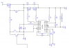
3) You should check the bulk capacitance requirements - each part usually has some recommendations as to how much capacitance they want. Altera probably has an app note on power supply circuit recommendations, plus it never hurts to put a couple 'C' or 'D' sized Tant. pads scattered around the board. Keep the ceramics though - they serve different purposes. The ceramics are located within a couple mm of the chip and supply the power for the switching spikes, while the larger Tant's filter power supply ripple and lower frequency stuff.

**broken link removed**
4) Dunno, don't use PICs much

5) Depends on who you ask... Electrically the voltage between them should be very close to 0, it's a question of noise at that point. I don't think it matters too much - but it doesn't hurt to make sure it's not sitting next to the switching regulator, and it's data lines to the FPGA are short and low capacitance.

6) On Xilinx parts anyway, clk lines are usually for clock inputs - any IO lines can serve as clock "drivers". After spending 10 min poking through the Altera docs, it looks like it's the same, but I'm not exactly sure.

7) If you have a 4 layer board, use the two inner layers for power and ground. If you have more internal layers, it's preferred to keep things paired up so that when currents flow, they have a good return path, as well as keeping the board symmetrical. Since this is based on a FPGA, you should be able to juggle the pinouts in order to make routing as simple as possible - most of the busses should be top-side without having to do any weird bends/flips.

Also pay attention to the example layouts for the switching regulators - follow them as closely as possible, and do copperfills/isolated ground "islands" as they call for.

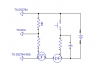
BTW, the DS2764 Sense line isn't wired up correctly - you should create another net called "BAT-" and wire that through the DS2764 instead of attaching the battery to Gnd.
 
kamdy said:
From the block diagram of the system you are using two buses I2C for the camera and the Fuel gauge and the SPI bus for the ADC and the LCD. I suggest using ADC and LCD with I2C bus instead of the SPI bus. This will minimize the number of pins and the software of the FPGA
I have made quite a bit of changes since I made the block diagram and one of the changes happened to be what you suggested. I no longer am using the SPI bus and I got rid of the ADC. (The LCD doesn't support I2C btw, so I would need some controller inbetween to go from I2C to parallel or SPI)

Thanks a ton for looking over my schematic hjames :). I have attached an updated version without the intenal sense resistor shorted. I'm glad you pointed that out. I'll prowl over the PSRAM datasheet a bit more to figure out what to do with the unused data lines. My guess is that I will leave the pins disconnected and tie the upper byte enable to high. Thanks again for your assistance!
 

Attachments

  • schematic3.pdf
    50 KB · Views: 205
freeskier89 said:
I have made quite a bit of changes since I made the block diagram and one of the changes happened to be what you suggested. I no longer am using the SPI bus and I got rid of the ADC. (The LCD doesn't support I2C btw, so I would need some controller inbetween to go from I2C to parallel or SPI)
The following URL might help
**broken link removed**
 
Last edited:
One other thing since this is supposed to be a portable device - power-on/soft-off is something that you should figure out how to implement. A simple PMOS pass transistor spliced into the VCC line, and a spare line (maybe replacing one of the switches you alread have). Another way is to jerry-rig all the enable lines of the power supply chips, but this would be trickier since the LM2704/boost converter is sitting directly on the VCC line.

Two other comments - have you looked into using LEDs instead of the flash tube? **broken link removed** I bought some from Future-active a couple months back, so I they should be pretty available. You might be able to charge some capacitors from the OLED power supply and just use it like that.

Also, https://www.electro-tech-online.com/threads/ftdi-vdip1-eval-kit.25544/
Seems to be a new chip out. This would significantly change your design, so I'm not sure if it's worth it or not.
 
hjames said:
One other thing since this is supposed to be a portable device - power-on/soft-off is something that you should figure out how to implement. A simple PMOS pass transistor spliced into the VCC line, and a spare line (maybe replacing one of the switches you alread have). Another way is to jerry-rig all the enable lines of the power supply chips, but this would be trickier since the LM2704/boost converter is sitting directly on the VCC line.
haha... I am so glad you pointed that out! I forgot a power switch. That would be bad to get the boards back and figure out that the device would always be on. Hmm... I am going to have to think on how I want to do that. What do you think of using a SCR and that is triggered by a single pushbutton for powerup, and then MCU would shut off power with a power NMOS. I attached a schematic. Is their a distinct advantage of using P channels?

hjames said:
Two other comments - have you looked into using LEDs instead of the flash tube?
Yes and no. This is where this device starts differing from a normal digital camera. If I could get ahold of some really powerful UV LEDs(ones that emit as much light as a normal mercury vapor blacklight) then I would be really really happy to use them, but the most I can find is a 200mW $300 Power UV LED from Nichia. That will obviously not work. I am planning on using a xenon flash tube and then running the light from that through a UV transmissive filter (section of a blacklight tube). If you happen to have any ideas regarding UV illumination I would be very happy to hear because, right now, that is the sketchiest part of the project.
Also, https://www.electro-tech-online.com/threads/ftdi-vdip1-eval-kit.25544/
Seems to be a new chip out. This would significantly change your design, so I'm not sure if it's worth it or not.
Oooo... That looks very nice. I wish I would have seen that earlier. Oh well, I think the current setup will be fine for now.

Edit... Considering the battery is only putting out 3.6V tops, I would imagine that a SCR would drop too much voltage, no? Its on-state resistance is much higher than a mosfet right? Maybe SR latch with mosfet at the output would be better.
 

Attachments

  • startup.png
    startup.png
    5.4 KB · Views: 292
Last edited:
Well, you'll need to decide whether you want to disconnect the DS2764 when you power down the device or not - it'll reset the battery capacity gauge when ig gets disconnected.

The main problem with using N-channel FETs is that disconnecting ground leads to some issues if you have to interface logic on the battery side... In any case, it's better to have the power switch temporarily trigger the gate of the pass mosfet - long enough for the PIC to override the switch and maintain power to the circuit.

400nm LEDs are available - $1 each, direct from the manufacturer...
**broken link removed**

Lumileds has a 600mW 460nm LED, which is definitely in the visible region.
Digikey used to carry some 370nm LEDs, but looks like they stopped.
 
hjames said:
Well, you'll need to decide whether you want to disconnect the DS2764 when you power down the device or not - it'll reset the battery capacity gauge when ig gets disconnected.

The main problem with using N-channel FETs is that disconnecting ground leads to some issues if you have to interface logic on the battery side... In any case, it's better to have the power switch temporarily trigger the gate of the pass mosfet - long enough for the PIC to override the switch and maintain power to the circuit.
True. That sounds like a good idea.
hjames said:
400nm LEDs are available - $1 each, direct from the manufacturer...
**broken link removed**

Lumileds has a 600mW 460nm LED, which is definitely in the visible region.
Digikey used to carry some 370nm LEDs, but looks like they stopped.
I need something that is 370nm or lower, and they need to be pretty powerful... I have tried an assortment of UV led's and they do not cut it. I might be able to put together an array of 365nm leds together though.

Thanks again for all of your help!
 
Does this look good for the power on circuit? The base of the npn transistor is connected to the mcu.

Edit: Hold on... my mosfet symbol is wrong... imagine the mosfet on the left is a p-channel not a n-channel.
 

Attachments

  • batterymon.png
    batterymon.png
    11.1 KB · Views: 346
Last edited:
It'll work, with two comments:
1) Make sure the Mosfet is plugged in so that the body diode is in the right direction
2) I usually like to hook it up so that the uC can sense the state of the switch - one way of doing this is to have the switch pull on the NPN's base through some resistors. The PIC can then poll the switch by temporarily switching the pin into input mode and seeing whether the switch is pulling the pin high or not.

Essentially: PIC -> R1 -> switch pull-up node -> R2 -> NPN's base
With one end of the switch connected between R1,R2, and the other end going to positive voltage rail.
 
Thanks for the info.

Alright I almost have all of the components layed out in an efficient manner on the board in diptrace. It is sure a time consuming process to lay everything out well, but it'll sure help when it is time to route it. I am going to check all of the IO pins on all of the ICs to look for open-collector/drain pins where I am missing pullups/pulldowns and then hopefully start routing. Is there anything else I should be looking for in my final check?

Out of curiousity, if I were to send off the board today and it conformed to schematic, what do you think are the chances that I have a critical error somewhere that impairs the functioning of the device? I am just curious what a person with a lot more design experience thought.

I cannot thank you enough for all of the time you have spent looking through my stuff... it is invaluable!

semi-off-topic: If anyone is looking for a great book on electronic design, I just got this one and it is absolutely splendid. It has great info about board/schematic design that I have never seen anywhere else! https://www.amazon.com/Circuit-Designers-Companion-Second/dp/0750663707
 
Usually I check the following things:
Connectors - messing up one of these can really mess up a board.
3 pin parts - mosfets/bjt's, especially since there isn't a standardized numbering scheme.
via's/test points on all the critical nets - they come in really handy when working around mistakes...
positive/negative logic - i.e. wiring the disable line of a regulator to vcc...
clearance/mounting issues - properly sized screw holes work better than ones that are too small. Ditto on fitting something into a box when it is a couple mils oversized.

Eyeball the layout to see if there are any missing pins that ought to be there - spend a couple minutes on each part, mentally tracing out what other parts it should be connected to. I tend to catch a couple of big gotcha's this way.

I think I've probably built somewhere around 100 different boards, and the number that have been completely free of issues is probably <25%. Obviously a lot of these are one-off test boards that are there for general fiddling around, but in general, bug free is pretty rare. The important part is to make sure you get something functional. I think I've only completely botched one of the boards - a breakout board where the connectors were just-plain-wrong.

As long as you have enough places to solder random jumpers, nearly everything is salvagable. Soldering jumpers on .5mm pitch TQFP's, lifting pins, milling out shorted pins, lots of cuts-and-jumps, oddball resistors and capacitors wedged into weird places - there are official manuals on how to do this stuff, and it happens a lot. It won't look pretty, but I aim for functional in the first iteration, pretty comes with version 2. Usually this means throwing in extra parts -extra LEDs and testpoints and jumpers, places for alternate components, anything that will make debugging easier.

And obviously there are the logic/design issues - double check the bandwidth numbers, maximum clock rates, voltages, currents, unexpected parasitic/protection diodes, interrupt latencies/jitter, memory sizes, etc. Messing up one of these will cause lots of grief later on.

Tricky part is that I've managed to stay away from BGA's - they really are expensive in terms of board cost and manufacturability. Plus undoing a mistake on them isn't possible, so you'll have to be doubly careful of them.
 
I will definitely insert some test points into the board. That sounds like a very wise idea. I must say that those VFBGAs are making me nervous, but I really don't have much of an alternative at this point. I could work with the added complexity of DRAM instead of PSRAM because they come in tsop packages, but I do not want to change the design now. Besides, I would still have to work with the camera.
 
Alright, I am back with more questions... I promise you that this project will be done sometime soon so the questioning should cease :)

Alright, the things I am currently worried about...

Battery Loading:
This is what I am working with:
https://www.electro-tech-online.com/custompdfs/2006/12/UnionBattery-860mAh.pdf
- First, Battery Life I am not concerned about... If it runs out in a half an hour that's fine with me.
- Second, what do you anticipate my FPGA will draw? It is a pretty small basic one... (EP2C5)
- What is a safe amount of current to draw from the battery?
- Won't my inductive charge pumps (LTC3441, LM2704) draw up to a half an amp at times? Am I interpreting the LM2704 datasheet wrong? If not, would a large capacitor (1000uF+) help so that it just draws out of the cap when the inductors are drawing the peak current.
- Am I interpreting the datasheet correctly when I see that 2A is the max I should pull out of the battery? If so, how much should I stay below that so that my battery does not go up in a bright white flash :)?
-Do you think that I will be fine for current consumption?
-I am 95% sure that I am not going to use the Xenon flash anymore. I found a new manufacturer (www.thefoxgroupinc.com) of 360nm UV LEDs with good output power. And they gave me 10 for free :). They have been the easiest electronic company to deal with! This will cut down current consumption and noise injection a lot.

I attached an image of the progress of the board in case you are interested. It is very very near completion... I just need to work out via sizes, copper pours, making traces as low impedence as possible, and make a couple more tweaks.

Edit: Hmm... I just emailed sunstone (pcbexpress.com/pro owner) regarding the vias between CSP pads and whether or not they could do it, and I got a reply consisting of a table I already saw pasted from their website. For the 8mil hole via, they require a 25mil pad. With a 25mil pad that gives me 1mil (2mils max) between the BGA pad and the via pad! Since it is just a via, can't the pad be a bit smaller? Do you recommend any other companies? I am currently looking into advancedcircuits, but it looks considerably more expensive.
 

Attachments

  • boardpreview.pdf
    97.2 KB · Views: 167
Last edited:
I'm not sure if I'd start off a project like this with the board design, as there are so many things that can change.

If you want to use the Cyclone-II, why not check out the DE1 development board? It gives you (IIRC) 76 user I/Os, plus a lot of other commonly-used chips / ports for about USD $150. For the $1400 that you mentioned, you could probably cover your whole design with eval boards, and start the firmware stage with known-working hardware.

Once you get your firmware made (which is going to be a WAY bigger project than the board design), you can just read-off the board connections from your pin assignments and the chip datasheets.

Also, if you want to use some kind of CPU in the design, why not check out the freely available cores? They come in all shapes and sizes (from PIC clones to the OpenSPARC), and can seriously cut development time. You have to be careful about the licenses, so your whole design doesn't end up GPL'd by accident, but if you're going after patents then you will be talking to IP attorneys anyway...
 
Well, im not using a bunch of dev/eval boards because the whole point in making the board was to show that it could be portable and low cost (component costs) and also so I could learn a lot from it. I think that the firmware will take some time, but I am a WAY better programmer than electical engineer. For that reason, I thought I would dwell on custom circuitry. I guess I do not see how using a core would cut development time. I would rather have the system be optimized to begin with rather than throwing something together that is rough and then trying to patch it up later.
 
freeskier89 said:
Well, im not using a bunch of dev/eval boards because the whole point in making the board was to show that it could be portable and low cost (component costs) and also so I could learn a lot from it. I think that the firmware will take some time, but I am a WAY better programmer than electical engineer. For that reason, I thought I would dwell on custom circuitry. I guess I do not see how using a core would cut development time. I would rather have the system be optimized to begin with rather than throwing something together that is rough and then trying to patch it up later.

Dev boards are designed to make it as easy as possible to reimplement your project on your own board (the vendor will even help you do it a lot of the time). If you get something working on eval boards, it's trivial to extract a schematic for the exact circuit you used without including any unused parts. Once you have the bill-of-materials and approximate board layout, you can call around and pull together a reliable mfg. cost estimate.

What you do with an FPGA is very different from programming a microprocessor. Instead of typing instructions that run in order, you're laying out registers and gates. When you write HDL code, you are literally designing a chip; the FPGA is one option for implementation, but the same code can be compiled into an ASIC.

As for IP cores cutting development time, you'd be amazed at what a little licensed material can do. If your project, for example, uses SD cards, USB, Bayer decoding, LCD screen, possibly a CPU, etc., each one of those items is going to be a royal PITA to get working. If you can go to opencores.org and pick up a few big pieces of your project under an LGPL license, then those steps just go away.
 
I am planning on doing all of those things such as usb, lcd, and sd on the PIC MCU, not a FPGA. Also I will be using a few interface chips to simplify it (FT232RL for usb and the DOSonChip FAT16/32 controller).I am well aware of the architecture of the FPGA, that is why I shifted to using a MCU for the sequential tasks, and I am only going to use the FPGA for image buffering (sending it off to PSRAM) and the basic edge detection and line recognition algorithms. Besides, it is far far to late to give up on a board that is nearly done.
 
Lithium batteries can usually be discharged at 1C with pretty good results (i.e. 1 hour run time). The main tradeoff is that the battery impedance causes a corresponding power/runtime loss. Doing hard pulses out of the battery probably won't damage it, but it may reduce the runtime considerably...

Each of the regulators should have enough capacitance in front of it (preferably low impedance tantalums) to smooth out the current spikes. If you're really paranoid, you can put pads for optional inductors in series with the battery connection to smooth it out even more.

The overkill way of doing the LED is to charge up a big capacitor, then disconnect the capacitor from the battery, and do the pulse directly from the capacitor. At the very least a current limiting resistor between the capacitor and the battery will keep things sane. The other thing is to design the circuit so that it can never lock "on" because of a firmware error.

As for the development kit stuff, it is a nicer way of starting things out. The common approach is to just put in enough connectors on your board to access the important stuff - the LED drive, the power connections, camera, IO, - you can use a mix of stuff from the devel kit and from your custom PCB during development.

If nothing else, someone's already done most of the high-risk BGA stuff for you, and you'll have a way out if you accidentally toast the BGA...
 
Thanks that helps! I contacted sunstone again, and they really only suggest going a couple of mils below the 25mil recommendation for the pad. If I push the via into the pad a bit (as shown in attachment) it will work, but... the whole reason for the 25 mil pad is that the drill may hit anywhere in that pad, and then the way I have it now, that would suck the solder out of the joint, no? Am I going to have to find someone who does laser vias?
 

Attachments

  • via.png
    via.png
    4.3 KB · Views: 143
Status
Not open for further replies.

Latest threads

New Articles From Microcontroller Tips

Back
Top