Dear all,
We have been assigned a bonus project that upon completion will reward us with an extra 20% on our grade! (yes crazy, but its definitely out of our league)
This is what the assignment handout reads:
--------------------------------------------------------------------------
1.1 DESIGN REQUIREMENTS
Design an amplifier with a minimum gain of 10 @ 10 KHz, minimum voltage swing of 5 volts (p-p) at the output, maximum output resistance of 1 kΩ, and minimum input resistance of 50 kΩ. You may use up to 2 transistors (e.g two 2N7000 MOSFETs or two PN2222 BJTs, or one MOSFET and one BJT). Make sure that you only use standard resistors. Use only one power supply with a voltage of 12 volts. Make sure the distortion is minimized (i.e. bias the transistors away from cut-off or triode/saturation). It is ok to have a design better than the specifications (e.g. gain > 10, or Rout < 1 kΩ). Simulate your circuit on Multisim BEFORE the lab session.
1.2 LAB WORK
a) Assemble your design in the lab. Measure and record the DC values of the voltages for all the nodes of your circuit. Estimate the currents.
b) Choose Vsig to be 250*sin(20000π t) mV (i.e. 500 mV p-to-p). Measure the AC output voltage. Plot the input and output signals on the same screen. What is the voltage gain Vo/Vsig? Compare it with your theoretical calculation.
c) Measure the input resistance by measuring the AC voltage of the base/gate and the input voltage Vsig. Compare it with your theoretical calculation.
d) Measure the output resistance by measuring the gain, once for a load resistor of 1 kΩ and once by measuring the gain without the load resistor. Estimate the output resistance based on the two measurements. Compare it with your theoretical calculation.
1.3 RESULTS
1) Measurements:
Measure the DC and AC voltages of all the nodes of the circuit. Measure the voltage gain Vo/Vsig, input resistance, and output resistance and compare them with your theoretical calculations.
2) Simulation:
Simulate your circuit on Multisim. Include the plots of input and output voltages in your report.
--------------------------------------------------------------------------
Just finished making a 1L coffee jug. I have been preparing for the past 2 hours on transistors (BJT and MOSFET's) and I still feel that I do not understand circuit examples that are presented. However, the most helpful and simplified reading I got my hands on was the following:
**broken link removed**
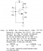
Correct me if I'm wrong but I think using 2 BJT's in the Common Emitter configuration would be the way to go on this.
Anyhow, How should I start tackling this problem?
Your input is greatly appreciated.
We have been assigned a bonus project that upon completion will reward us with an extra 20% on our grade! (yes crazy, but its definitely out of our league)
This is what the assignment handout reads:
--------------------------------------------------------------------------
1.1 DESIGN REQUIREMENTS
Design an amplifier with a minimum gain of 10 @ 10 KHz, minimum voltage swing of 5 volts (p-p) at the output, maximum output resistance of 1 kΩ, and minimum input resistance of 50 kΩ. You may use up to 2 transistors (e.g two 2N7000 MOSFETs or two PN2222 BJTs, or one MOSFET and one BJT). Make sure that you only use standard resistors. Use only one power supply with a voltage of 12 volts. Make sure the distortion is minimized (i.e. bias the transistors away from cut-off or triode/saturation). It is ok to have a design better than the specifications (e.g. gain > 10, or Rout < 1 kΩ). Simulate your circuit on Multisim BEFORE the lab session.
1.2 LAB WORK
a) Assemble your design in the lab. Measure and record the DC values of the voltages for all the nodes of your circuit. Estimate the currents.
b) Choose Vsig to be 250*sin(20000π t) mV (i.e. 500 mV p-to-p). Measure the AC output voltage. Plot the input and output signals on the same screen. What is the voltage gain Vo/Vsig? Compare it with your theoretical calculation.
c) Measure the input resistance by measuring the AC voltage of the base/gate and the input voltage Vsig. Compare it with your theoretical calculation.
d) Measure the output resistance by measuring the gain, once for a load resistor of 1 kΩ and once by measuring the gain without the load resistor. Estimate the output resistance based on the two measurements. Compare it with your theoretical calculation.
1.3 RESULTS
1) Measurements:
Measure the DC and AC voltages of all the nodes of the circuit. Measure the voltage gain Vo/Vsig, input resistance, and output resistance and compare them with your theoretical calculations.
2) Simulation:
Simulate your circuit on Multisim. Include the plots of input and output voltages in your report.
--------------------------------------------------------------------------
Just finished making a 1L coffee jug. I have been preparing for the past 2 hours on transistors (BJT and MOSFET's) and I still feel that I do not understand circuit examples that are presented. However, the most helpful and simplified reading I got my hands on was the following:
**broken link removed**
Correct me if I'm wrong but I think using 2 BJT's in the Common Emitter configuration would be the way to go on this.
Anyhow, How should I start tackling this problem?
Your input is greatly appreciated.
")