Electro Tech is an online community (with over 170,000 members) who enjoy talking about and building electronic circuits, projects and gadgets. To participate you need to register. Registration is free. Click here to register now.
Welcome to our site! Electro Tech is an online community (with over 170,000 members) who enjoy talking about and building electronic circuits, projects and gadgets. To participate you need to register. Registration is free. Click here to register now.
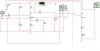
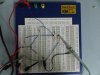
Ok guys, sorry I haven't read the last couple of replies but here is what ive done so far. The labs are closing now so Ill post a schematic of what ive done and will go through the previous posts and try to learn.
The problem here is stage two. Stage one works perfectly.
I removed all the wires for your 'scope and cropped your schematic.
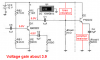
The output transistor is missing a bias resistor and an emitter resistor.
The emitter of Q1 has a voltage too high at 4.9V and a collector too low at 6V. Then its max swing is only 1.1V p-p which is reduced to 0.55V p-p by Rload (1k).
The voltage gain is about only 3.9.
The input impedance is about only 3.7k ohms.
Audioguru is right, just use the MOSFET as your input stage and you don't have to worry about the input impedance specification, as it will definitely be way higher than 50kΩ.
My gut instinct tells me MOSFET in common-source configuration as your input stage. You should be able to get a decent gain out of this, definitely higher than 10. As for the second stage, I would first try a source-follower or emitter-follower. This will ensure that your output impedance is low. You are given 12V supply voltage and only need to hit 5V swing on the output, so you barely have to worry about that, just play with your DC biasing to get the DC output voltage near 6V.
slightly off topic, as honestly I am not competent in anything analog,
Does the R2+R4,R3 voltage divider (in DC mode) provide some kind of gate biasing to get the mosfet in the linearish behaviour zone. Wouldn't that be quite variable between mosfet even of the same designation? As I understand, mosfets have a relatively small useful linear band, mostly around the inflexion point in the middle of the transfer graph.
The capacitor decoupled input makes the gate variate in the zone, hence getting the DS resistance to change.
But then, is it not risky to have the gate biased by an essentially input dependant voltage.
As I understand, this is then controlling the voltage at the base of the bjt, effectively dividing the current between base current and trough mosfet current. Essentially this is creating a current source somehow proportional to the AC input. I still do not completely see why R4 doesn't go straight to VCC if my undertanding of the circuit is correct.
If anyone could explain to me a bit more how this all goes, I would be most grateful.
If no one feels like it, it is also perfectly acceptable.
Did you look at the datasheet for the 2N7000 Mosfet? Its gain (transconductance) is a wide range. There are low gain ones and there are high gain ones. You must bias it using negative feedback for a low gain one to work as well as a high gain one.
When the gate resistor connects to the drain then when a low gain Mosfet does not conduct much then the drain voltage is higher and it feeds more voltage into R4 which turns on the Mosfet more.
When a high gain Mosfet conducts too much then the drain voltage is lower and it feeds less voltage into R4 which turns on the Mosfet less.
If you bias the Mosfet with a voltage divider from the supply voltage then a low gain Mosfet might be turned off and a high gain Mosfet might be turned on too much.
the way to get the proper bias on the MOSFET and keep a high input impedance is to isolate the voltage divider from the gate with a high value resistor. all you need here is a voltage. the Mosfet gate capacitance which is a maximum of 50pf has an impedance of 3Meg at 10khz. so you can use a 100k isolation resistor to connect the voltage divider, and your input impedance will be just a little below 100k. this can be done with MOSFETs and tubes, but not with bipolar transistors. look at my example above. or use audioguru's self biasing scheme, and you won't have to tweak the bias network. looking at the Fairchild data sheet, the production range for Vgs(th), the gate threshold voltage is from 0.8 to 3.0V. that's a very large range, and audioguru's self biasing scheme might work best with this device. you want to eliminate the actual device tolerances as much as possible and let physics do the heavy lifting. the goal here is for a circuit to work first time, every time. of course life is full of surprises, but that's the goal to shoot for.
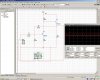
After fiddling with the circuit for quite some time, I managed to get all the requirements done. Gain of 11x, a sky high input impedance (100K) and a weird output impedance of 348 ohms.
However, this 348 ohm output impedance was acquired after waiting for 2 minutes in simulation on the multimeter. It was weird, the value kept going up and down, but the general trend was decreasing, i.e:
1Mohm --> 500kohm --> 800kohm --> 300kohm --> 600kohm --> 100kohm... until eventually I caught it at 348ohm and paused it!
In joy, I call my professor to show him the circuit.Turns out that 'feedback' circuits are REALLY out of our league and that we shouldn't use them unless we fully know what we are doing. According to him, if we implement it on the breadboard and something goes wrong, we(I) really cant do much about it since we don't know how feedback circuits work inside out.
Good news is that he postponed the deadline for another 2 weeks so plenty of time for me to learn more about 2-stage amplifiers and fiddle some more. Problem is we have a 10 day holiday in which the university is closed, that means no MultiSim for me. I am downloading the trial edition(proffesional version) from their website as I write this, but I own a macbook. How harsh is multisim on a 1 year old Fijitsu-Siemens laptop? Will it be able to run it properly?
As for creating a non-feedback circuit, I think I should start from scratch using a Common-emitter for stage 1 and an emitter follower for stage 2. Or should I just stick with 2 MOSFETs? (someone in my class did it perfectly with 2, 2N7000 MOSFETs.
d) Measure the output resistance by measuring the gain, once for a load resistor of 1 kΩ and once by measuring the gain without the load resistor. Estimate the output resistance based on the two measurements. Compare it with your theoretical calculation.
Personally I would have written it like this:
Measure the output resistance by measuring the output level, once for a load resistor of 1 kΩ and once by measuring the output level without the load resistor. Estimate the output resistance based on the two measurements. Compare it with your theoretical calculation.
another way to measure output impedance (in a sim) is to feed a known AC current at the frequency of interest into the output terminal of the amplifier (since you're looking for 1k or less, 1mA AC at 10khz will do it) with no input signal (put a ground at the input side of the input cap instead of applying a signal there), and read the resulting voltage developed at the amp output terminal. with 1mA fed into the output terminal, the voltage will be 1V/kΩ. that's the quick way to verify the output impedance. after you get it where you want it, verify it with the method given, i.e. the difference in output voltage loaded and unloaded.
@audioguru: That's a good question. This same setup would probably not work since its not a generic setup. For different MOSFET's, won't you just bias it accordingly?
@sceadwian: Take it easy on me I'm still new in the field of electronics I spaced them out so it can be simpler for me to visualize things.
This site uses cookies to help personalise content, tailor your experience and to keep you logged in if you register.
By continuing to use this site, you are consenting to our use of cookies.