Continue to Site

Welcome to our site!

Electro Tech is an online community (with over 170,000 members) who enjoy talking about and building electronic circuits, projects and gadgets. To participate you need to register. Registration is free. Click here to register now.

  • Welcome to our site! Electro Tech is an online community (with over 170,000 members) who enjoy talking about and building electronic circuits, projects and gadgets. To participate you need to register. Registration is free. Click here to register now.

Reducing power supply for a PCB containing FTDI FT232

Status
Not open for further replies.

nickagian

Member
Hi!

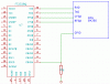
I have a PCB that (among other electronics) contains a EM250 ZigBee module connected over the UART interface with a FT232 FTDI IC, as shown in the second attached figure.

The problem is that due to this connection the power consumption of the PCB is higher than I expected. The FTDI is power from the USB bus (and not from the power supply of the PCB) which is however not all the time present. Thus, I assume that the high power consumption that is measured only when the USB supply power is not present comes from current throwing from/to the pins of the EM250 to/from the pins of the FT232. I have tried all possible states of the pins of the uC but could not go too low in the power consumption (the best is around 700uA, while around 200uA was expected).

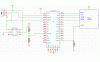
To reduce the power consumption further, I was thinking of making the modification shown in the first attached figure, thus adding some buffers between the two ICs that are going to be activated only when communication is required (when the USB supply power is actually present) and remain deactivated otherwise.

Do you think that this will work? Do you have any other alternative to propose me?

nikos
 

Attachments

  • ftdi_mcu-current.GIF
    ftdi_mcu-current.GIF
    20.2 KB · Views: 321
  • ftdi_mcu-new.GIF
    ftdi_mcu-new.GIF
    16.5 KB · Views: 334
Last edited:
Fairly obviously if you switch any output lines feeding the FTDi chip to ground, then no current can flow that way - and if you ground any input lines (just to test it) then that will prevent any possible CMOS input problems (assuming your processor is liable to such problems?). If that doesn't reduce the current, then it's not a problem with the FTDI chip - and you need to look elsewhere.

Have you tried it with the FTDI chip removed?, try that and see what you measure.

Certainly in my experience it's VERY, VERY hard to approach the claimed consumption figures.

I've just this morning started running consumption tests on my PIC GSM project (as the prototype has gone off to be demonstrated) using just a PIC, with nothing connected to it.

This is a nano-watt device, supposedly one of the lowest consumption devices available.

Using a simple endless loop, and running at 4MHz (using the internal oscillator) it takes 1.02mA from 3.6V

Dropping down to 31.5KHz, consumption drops to 560uA (I was expecting a MUCH larger drop than that).

Putting the device to sleep drops consumption down to 150uA.

I only did very brief tests, next I'm going to try shutting peripherals down see what effect they have - although (I think?) the only one I have setup is the USART - I'm not sure if any other peripherals are actually running by default or not.
 
I'm sorry Nigel, I haven't understood your suggestions, that first part of your post talking about switching the lines to ground. You mean to switch all UART lines between the two chips to ground? But how to do that? By driving them from the uC to output direction and LOW state? There are some input lines, going into the uC, as well. What should I do with them?

Anyway, the problem seems to come from the fact that when I put the processor in sleep, the FTDI is not powered at all. Something very weird happens in that time periods inside the FTDI. When I plug the USB cable and the FTDI gets power, the consumption is much lower. That's why I believe that the FTDI is the source of the 'problem'.

Moreover, I have noticed a behaviour like that with a flash memory. The current consumption when the device was powered-down, caused by current flowing through the pins of the uC, was higher than the case where the device was in power. It may sound weird, but I have seen that in practise.

And have in mind that indeed I have removed the FTDI and the consumption falls to the levels that I mentioned. I also have another design with the same uC that can achieve that levels of power consumption (~200uA).

I completely agree with what you mention lower in your post. That 200uA is totaly higher than the number stated in the datasheet of the processor.

Perhaps my idea of putting some buffering or switches between the two ICs is not very conventional, but I am trying to think of a way to reduce the consumption as much as possible. :)
 
I'm sorry Nigel, I haven't understood your suggestions, that first part of your post talking about switching the lines to ground. You mean to switch all UART lines between the two chips to ground? But how to do that? By driving them from the uC to output direction and LOW state?

Yes, exactly that.

There are some input lines, going into the uC, as well. What should I do with them?

Solder a temporary wire down to ground from each input pin.

But just do the outputs as above first.

Anyway, the problem seems to come from the fact that when I put the processor in sleep, the FTDI is not powered at all. Something very weird happens in that time periods inside the FTDI. When I plug the USB cable and the FTDI gets power, the consumption is much lower. That's why I believe that the FTDI is the source of the 'problem'.

Moreover, I have noticed a behaviour like that with a flash memory. The current consumption when the device was powered-down, caused by current flowing through the pins of the uC, was higher than the case where the device was in power. It may sound weird, but I have seen that in practise.

And have in mind that indeed I have removed the FTDI and the consumption falls to the levels that I mentioned. I also have another design with the same uC that can achieve that levels of power consumption (~200uA).

I completely agree with what you mention lower in your post. That 200uA is totaly higher than the number stated in the datasheet of the processor.

Perhaps my idea of putting some buffering or switches between the two ICs is not very conventional, but I am trying to think of a way to reduce the consumption as much as possible. :)

That's massive overkill, and really a very poor solution :D

I'm assuming you're leaving pins output HIGH on the processor?, which would be the default position if you're leaving the UART running. If the FTDI chip has protection diodes?, then it will power itself via those protection diodes.

Curing it 'may' be as simple as disabling the UART?, but disabling it and setting the pins LOW should prove it quite easily.
 
Yes, exactly that.

Solder a temporary wire down to ground from each input pin.

But just do the outputs as above first.

That's massive overkill, and really a very poor solution :D

I'm assuming you're leaving pins output HIGH on the processor?, which would be the default position if you're leaving the UART running. If the FTDI chip has protection diodes?, then it will power itself via those protection diodes.

Curing it 'may' be as simple as disabling the UART?, but disabling it and setting the pins LOW should prove it quite easily.

Well, unfortunately I didn't see any light.

What I have done is to disable completely the UART module inside the uC during sleep and to put all output pins to LOW.

However, nothing new has been noticed. The power consumption was as high as before.

There is no way that the power consumption comes from anything else on the board, because the problem is solved when I remove completely the FTDI chip. I have attached my complete design regarding the FTDI.

Is it possible that something is cause by that protecting diodes between the USB plug and the FTDI? I should try to remove them and see what's happening.
 

Attachments

  • ftdi_mcu-design.GIF
    ftdi_mcu-design.GIF
    14.6 KB · Views: 275
Well, just to update you. I've solved the issue.

The secret was that during sleep, the internal UART module of the uC should be deactivated and the relevant pins (TXD, RXD, RTS, CTS) should be configured at input direction with no pullup/pulldown. With this settings, I have managed to achieve the lowest possible current consumption (~100uA).

Nigel, I'm really curious. I also thought that it was better to configure the pins as outputs and at LOW state. Do you have any explanation that in the end the above described configuration should be used? I really cannot understand it exactly.

Nigel (and ronv), thank your very much for your help and your time, anyway.

Regards, Nikos
 
Nigel, I'm really curious. I also thought that it was better to configure the pins as outputs and at LOW state. Do you have any explanation that in the end the above described configuration should be used? I really cannot understand it exactly.

Did you check the voltages like I asked?.
 
Did you check the voltages like I asked?.

Nigel I'm sorry, I had forgotten to reply to that question.

In fact, I had configured the outputs to LOW state and then measured the voltages on these pins. Well, it was a little weird. Sometimes it was 0 and then some other times it was HIGH. And I think that this had something to do with the RESET state of the FTDI. And whether I had previously connected the USB plug or not. In fact, I had read in some application note of the FTDI for some previous version of the chip that during reset the output pins (from the side of the FTDI) were pulled-up weakly. I had the same problem in a previous design too. I had tried then all combinations for the uart pins (outputs with HIGH/LOW, inputs with pullup/pulldown etc.) but in the end my mistake was obviously that I didn't disable the UART at the uC.
 
Status
Not open for further replies.

Latest threads

Back
Top