Electro Tech is an online community (with over 170,000 members) who enjoy talking about and building electronic circuits, projects and gadgets. To participate you need to register. Registration is free. Click here to register now.
Welcome to our site! Electro Tech is an online community (with over 170,000 members) who enjoy talking about and building electronic circuits, projects and gadgets. To participate you need to register. Registration is free. Click here to register now.
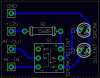
This is a typical example of "How not to design a PCB".
You're using the wrong layer for the traces. Using the bottom layer (16) for traces and the tPlace layer (21) for components you'll obtain a "look through the board" image. Using the top layer for traces you'll have to solder components from the component side, which is impossible since the solder pads will be obstructed by the part itself.
Using a double sided board with plated through holes the board is easier to populate and solder.
Further there are lots of acute and odd angles in the traces which will most likely lead to unsatisfactory etching results.
Last not least there are components overlapping each other from their size. How are you going to place those properly?
Why didn't you refer to my PCB design? I guess the PCBs are also smaller than yours.
its because your PCBs provided seem cant been edit , some trace are wide , some trace are small ... and my college printer seem cant support to print it... that why i redesign it ....
there wont be overlapping on component, because i was using more larger component's size to design , this is why my design is bigger than yours ....
for the switch , is this leave the no2 no connection?
its because your PCBs provided seem cant been edit , some trace are wide , some trace are small ... and my college printer seem cant support to print it... that why i redesign it ....
The images provided here were *.gif files. You can't use them to create a board for two reasons: they are not to scale and they have the components. A PCB layout should be printed having the dimension layer (20) the bottom layer (16) and the pads layer (17)
there wont be overlapping on component, because i was using more larger component's size to design , this is why my design is bigger than yours ....
DTDP switch got many type? My DTDP switch is ON, OFF, ON .... when supply to mid(2 & 5) , switch left to on LED on right , Switch right to on LED on left....
and about the circuit.... it only function 1 side , mean when speak on slave's mice, master's speaker voiced .... but when speak on master's mice, slave speaker is silent....
DTDP switch got many type? My DTDP switch is ON, OFF, ON .... when supply to mid(2 & 5) , switch left to on LED on right , Switch right to on LED on left....
but if i follow the connection provided, the D1 (silent) cant light up but its just a small problem , the main problem is the circuit can't function well
but if i follow the connection provided, the D1 (silent) cant light up but its just a small problem , the main problem is the circuit can't function well
1)i want to ask , what the purpose of 2.2k ohm resister (R5)
2)the IC is easy get hot after speak, after making the shielded container , the problem can be solved?
3)when speak at mice 1, the voiced out from speaker 2 is not as loud and clear as when speak at mice 2 to speaker 1, any solution can improve it ??
i was exactly follow the original circuit now , although the speaker 2 is not clear enough but everything is still work well.... just the IC temperature increasing after voiced out....
Do you have a TDA7052 or a TDA7052A?
What is the supply voltage?
What is the speaker impedance?
Was the amplifier running a continuous loud tone for a long time?
hmm.... i think 6V is not enough to support loudly voice.... how many ohms for the speaker i needed to 12V supply? or maybe can try the heatsink as the datasheet listed....
With a 6V supply and an 8 ohm speaker the output power is 1W to 1.2W which is much louder than a cheap clock radio. A door phone is used when the person is directly in front of it so it does not need to be loud.
With a 12V supply then 1W or 1.2W is produced into a 32 ohm speaker.
The datasheet says that with a 6V supply and an 8 ohm speaker then no heatsink is needed.
How can you add a heatsink? It is not made to use a heatsink.
This site uses cookies to help personalise content, tailor your experience and to keep you logged in if you register.
By continuing to use this site, you are consenting to our use of cookies.
")