DirtyLude
Well-Known Member
Mark,
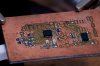
You showed me three examples of 20 mil traces. There is no components with 10 or 8 mil pads and all these traces look to be the same size as the pads so again .020" is the minimum reasonable size for thermal transfer, which is the width of the smallest pads. I have included a photo of what I am talking about. This is a snapshot of ExpressPCB with three of the smallest components and the smallest pads. The pads line up nicely with 20 mil traces. Do you disagree? can you prove to me where your 10 mil traces are again. And no those also are not 8 mil traces. Again the smallest pad is 24 mil. so your traces should be much smaller than the smallest pad.
The good news is the photo transfer method just using the sun and the same laser output with Pulsars foil can achieve 6 mils without a problem which again is an industry standard as the minimum for PC boards.
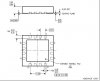
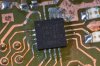
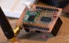
Your mistake is thinking that I'm using 0.05" lead spacing IC's. Your image shows spacing relative to a 0.05" lead pitch IC. The IC's on my boards are 0.5mm. If I used 20mil traces then there would be no space between the traces at all. 0.5mm is about 19mil length. The 8mil trace image is using an IC with 0.4mm lead spacing, that's less than 16mils from centre lead to centre lead.
I've been doing this for quite a while now. Try to assume I know the basics like the difference between 10 and 20 mil.