mvs sarma
Well-Known Member
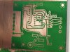
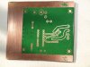
Whether the refurbished Toner cartridges like HP88A etc as in HP P1007 laser printer,would suit the TTS method? I suspect that they might not use Plastic powderYes I think you are right.
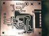
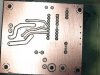
There is a something I read about using silk screening but with out poking holes in it but instead oil to wet the paper set it up on the photo resist and put it in the sun for 15 minutes. I wonder if that same concept would work with PC boards. I have plenty of old photo resist boards. This gets away from the vagaries of heat (yes the toner fuses at 275 to 290 °F and good luck finding anything that can control that tightly) and pressures that can move the traces (doubled sided trouble).
I've always liked the photo resist method and I wonder if going through the pin holed toner traces and through the oiled up paper that it fills in those pesky pin holes. Yep I think it is high time to try that.