Electro Tech is an online community (with over 170,000 members) who enjoy talking about and building electronic circuits, projects and gadgets. To participate you need to register. Registration is free. Click here to register now.
Welcome to our site! Electro Tech is an online community (with over 170,000 members) who enjoy talking about and building electronic circuits, projects and gadgets. To participate you need to register. Registration is free. Click here to register now.
Hi Eric, thanks for the reply. Newbie alert, please expand on "differentiated pulse" please!! Does this mean they introduce some external dead time reducing the chance of both FETs ever being on together? I am finding the signal level with the 1000pF caps is very low at the driver chip, only JUST enough to drive it reliably. For example, if you just touch pins 10 or 12 on the IR2110 when running the waveform to the gates goes berserk and stays that way. I found out by accident, then looked at the levels. Before C1 and C2 the levels are fine. Thanks again.
OK, thanks a lot for taking the time and trouble to simulate this, I just had a look on my scope at the inputs to the driver and there's a good similarity in the traces, I am impressed!
But in my naivety I have to ask just what do you believe the designer's intention was with these? Are they to add a period of dead time between switching the push pull output FETs, or what? I see capacitively coupled driver to gate configurations to stop a faulty signal holding a FET permanently on by blocking DC, but this is the first time i have seen caps *BEFORE* the driver IC. Thanks again, and thanks to AnalogKid for the Wikipedia link
Thanks again Eric, what i don't get, if that's their intention, is how it would work. Surely if it worked as a delay it's delaying both the same amount of time, so potentially they could still switch on at the same time. Wouldn't one have to be a different value to the other?
Thanks again Eric, what i don't get, if that's their intention, is how it would work. Surely if it worked as a delay it's delaying both the same amount of time, so potentially they could still switch on at the same time. Wouldn't one have to be a different value to the other?
hi,
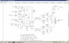
Assume that the IR2110 detects a 'high On' when the input signal is at say +2.5V and above level, the other input will be lower than 2.5v and can be considered as Off and Vice Versa on alternate phases.
The pins 10,12 are sensitive to the drive level of 74F74 since TTL only sources 2.5V @ 2mA ( yet sinks 20mA~0.5V).
So if you are using these obsolete TTL chips a 470Ohm pullup on pins 2,6 and 5 of FF are needed. Then the C1,2 values may need to be reduced.
Also pin 11 is high impedance and touching 12 or 10 with 11 shuts down the chip making the signals haywire, soa pull down R of 10K improves immunity on pin 11 (SD); (>100k to gnd internal)
But if you are using 74HC74 then you should be getting 5V positive pulse with the negative pulses clamped by internal ESD diodes.
So this design has some minor flaws or sensitivities.
The intent is to drive the FF with 2x frequency then divide by two using Qbar to D feedback to get near perfect symmetry square wave.
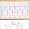
Each complementary output is differentiated so the rising output edge is the only active time each driver outputs are ON thus controlled by the RC decay time and thus the dead time, between one input going below Vih threhold to Vil and the other input fast rising edge.
Dead time ~0.5 us or so is typical and depends on power driver RdsOn and hence Coss. turn off delay.
1000pF and 15k yields a 15us time constant but since the threshold is near Vcc/2 it switches much earlier than this time constant for low pulse heights. This is not a precise method of deadtime control but I suppose can be made to work.
It is a classic problem with push-pull transistors to make sure that both transistors do not conduct at the same time- bad for the transistors, bad for the transformer, bad for power efficiency, and bad for output waveform purity.
The upper two NMOSFETs operate in parallel as do the two lower NMOSFET pair, so each parallel pair can be considered to be one bigger NMOSFET
As the other members have implied, and as you suspect, the diode in parallel with the 10 Ohm resistor turns the NMOSFETS on relatively slowly and off fast.
But, in order to understand how this works, you need to know one vital bit of information about MOSFETs: they have a very high gate/drain capacitance.
In order to charge and discharge the gate capacitance fast, a gate driver chips are used, as is the case in your circuit, Gate drivers have a high source and sink current capability, typically 1.5A.
Now to the core point; the the gate capacitance is charged up via the 10 ohm resistor (turn on) and is discharged via the 10 Ohm resistor in parallel with the forward biased diode, which could have a forward effective resistance of 0.5 Ohm.
So after all that, the you can see that the turn on gate time constant is 10 ohms * CGD (capacitance, gate/drain) and, roughly speaking, the turn off gate time constant is 0.5 ohms * CGD, ie 20 times faster.
That is not the whole story about gate driving, but I hope it answers your question.
Some great info, thanks. spec, I was asking about C1 and C2, but thanks for the info re gate capacitance. I am also aware that with paralleled devices the driver has to work twice as hard, I believe?
Eric, thanks for the revised simulation, again, appreciated!
Tony, I have just tied the shutdown pin 11 to ground with a 10k. Thanks. I also tried two off 470 Ohms resistors between the 5V pins 1, 4 and 14 and pins 2 and 6 and pin 5. With power applied and no signal I saw circa 5V on the pin 5 side of one resistor, and less than 1V on the pins 2 and 6 side of the other 470 Ohms resistor. Feeding a signal in saw noisy gate and drain waveforms compared to no pull ups. My issue with this is when a signal stops I often get a blown FET, sometimes, but very very rarely, I get it when a signal starts. The input waveform when looked at with a single shot on the scope, doesn't start clean, it "stutters" into life, but I don't have much if any control as it originates in my commercially made transceiver....
Ideas welcome, it's at times like this thermionic tubes seem appealing
I was asking about C1 and C2, but thanks for the info re gate capacitance. I am also aware that with paralleled devices the driver has to work twice as hard, I believe?
Yes, that is true about the gate driver having to work twice as hard with two parallel MOSFETs, but if you substituted a single MOSFET with twice the power capability, the gate capacitance would be liable to be twice as much so the amount of work the gate driver had to do would be around the same.
back to your original question about the Rs and Cs.
The resistors and capacitors form differentiators with a time constant of R * C.
The time constant is so long relative to the signal coming from the 74F74 that differentiation will not take place at the signal half periods, so the R and C combination will neither speed up or slow down the signal. They will simply make the mean level of the signal feeding the MOSFET driver zero volts (DC blocking).
But what the R/C combination does do is to switch off both MOSFET pairs, after a delay proportional to the time constant, if the clock input to the 74F74 is absent for any reason. This will protect the MOSFETs, transformer, and possibly other components, from excess current.
Why should one of the MOSFET pairs be permanently on if the signal were missing. The 74F74 has only two states and in one of those states, either Q or /Q output will be at a high level so, if the outputs of the 74F74 were directly coupled to the MOSFET driver inputs, one of the MOSFETs would be permanently on.
Why should a permanently on MOSFET damage itself and/or the transformer. A transformer has a primary inductance and is similar to an inductor. It is a characteristic of inductors that the amount of current flowing through them is dependent on the voltage across the inductor and the time that the voltage has been applied.
For example, if you had a perfect one Henry inductor and applied one volt across it from a perfect voltage source, the current through the inductor would increase linearly from zero amps at the rate of one amp per second without limit. So after an hour, for example, the current would be 3,600A.
But there is a further problem with practical inductors (transformers), after a certain current in the primary the core will saturate and you will no longer have an inductor but a piece of wire with a relatively low resistance. So, when the core saturates, the current shoots up and inevitably destroys some component, normally the transformer and/or the MOSFETs.
hi Chris,
If the frequency source waveform is not 'clean and sharp', the 7474 output could 'chatter' high/low on the slowly rising input clocking source.
I would consider squaring up the source waveform by using a simple filter followed by a Schmitt input, a 74HCT132 has a Schmitt input.
By using the second gate input on the 74HCT132, it would be possible to inhibit the clocking source to the 7474 during power up.
Eurika- that is probably the main operational reason for the Rs and Cs: to protect the circuit during power-up when, initially, the signal may not be present.
The signal to the IR2110 will always be present at power up, dependent on the state of Q or /Q of the 7474, at power up.
That is the purpose of the AC coupling from the 7474 to the IR, via C1/2
The signal to the IR2110 will always be present at power up, dependent on the state of Q or /Q of the 7474, at power up.
That is the purpose of the AC coupling from the 7474 to the IR, via C1/2
This site uses cookies to help personalise content, tailor your experience and to keep you logged in if you register.
By continuing to use this site, you are consenting to our use of cookies.

") Does this mean they introduce some external dead time reducing the chance of both FETs ever being on together? I am finding the signal level with the 1000pF caps is very low at the driver chip, only JUST enough to drive it reliably. For example, if you just touch pins 10 or 12 on the IR2110 when running the waveform to the gates goes berserk and stays that way. I found out by accident, then looked at the levels. Before C1 and C2 the levels are fine. Thanks again.
Does this mean they introduce some external dead time reducing the chance of both FETs ever being on together? I am finding the signal level with the 1000pF caps is very low at the driver chip, only JUST enough to drive it reliably. For example, if you just touch pins 10 or 12 on the IR2110 when running the waveform to the gates goes berserk and stays that way. I found out by accident, then looked at the levels. Before C1 and C2 the levels are fine. Thanks again.