Continue to Site

Welcome to our site!

Electro Tech is an online community (with over 170,000 members) who enjoy talking about and building electronic circuits, projects and gadgets. To participate you need to register. Registration is free. Click here to register now.

  • Welcome to our site! Electro Tech is an online community (with over 170,000 members) who enjoy talking about and building electronic circuits, projects and gadgets. To participate you need to register. Registration is free. Click here to register now.

Voltage-to-Frequency Converter II

Status
Not open for further replies.
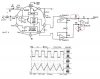
I need to see scope waveforms of the voltages on the input to the IA. To minimize loading, use a large-value cap in the V-F converter (like 100nF), and run the input voltage near maximum. Post the waveforms.
BTW, what is the input voltage you were using on the previously posted waveforms?
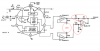
 
hey Ron a bit of doubt

In the latest posted waveforms, the time constant seems very low. Resulting in voltage rising too fastly. If he increases the capacitor value, then he can get a better waveform rite ?
 
krishnakanth said:
hey Ron a bit of doubt

In the latest posted waveforms, the time constant seems very low. Resulting in voltage rising too fastly. If he increases the capacitor value, then he can get a better waveform rite ?
I don't know what capacitor value he is using. Small cap values are OK in the final circuit, but scope probe loading is a problem, since a 10X probe is usually 10 to 15 pF. I just want him to use a large cap value so he can probe the cap without affecting the waveform too much.
 
Ok, i used C=100nF.

The 1st figure shows the waveforms on the input to the IA. The 2nd figure is
the square and triangle output.

Op-Amp supply voltage: +9V & -9V, V/F supply = 8 to 9V, V/F input = 4 to 5V

The results is still the same i think.
 

Attachments

  • Acrosss_diff.JPG
    Acrosss_diff.JPG
    42.6 KB · Views: 191
I still can't figure out why you get the distortion in the triangle. Can you post your most recent IA schematic, with all component values (including op amps)?
 
OK.

The Op-Amp supply voltage is +9 and -9V.

Is it because of the Op-Amps Slew rate? In the application notes, it did mentioned that high slew rate op amps are important.
The TL082CN and TL082CP i used has a slew rate of 16V/µs & 13V/µs. But in the application notes Figure 21 (**broken link removed**, AD712 has a slew rate of 16/µs, and AD711 has a slew rate of 20V/µs.
 

Attachments

  • VFC.JPG
    VFC.JPG
    34.2 KB · Views: 250
Last edited:
I can only believe that you have a wiring or component value error(s) in your circuit. Slew rate should not be a problem.

This probably won't solve your main problem, but you have some questionable values in your schematic:
1. The pullup resistor on pin 9 (330) is too low. The datasheet only guarantees 20mA sink current (10mA for the -SD and -SH versions). You are sinking 27mA.
2. I couldn't find a spec for the reference current (set by Rcal and Rscale), but the nominal is 1mA full scale. With 5V in, you are running more than that. Probably not a problem, but why risk it?
3. In the IA, I would go back to the original resistor values (all 10k except for the gain set resistor). If you need more output voltage, you could change the values of R17 and R19 to 20k (with R16 and R18=10k, as before).
 
The "gain" resistor does nothing in this circuit with the triangle wave output except load down the 1st opamp. The two signals to the IA are not differential, they just alternate from one input to the other input.
The ramping signals to each input show as about 2V p-p and each input of the IA has a gain of 0.5 so the triangle wave output should be about 1V p-p but measures only 0.1Vp-p.
 
audioguru said:
The "gain" resistor does nothing in this circuit with the triangle wave output except load down the 1st opamp. The two signals to the IA are not differential, they just alternate from one input to the other input.
True, but to clarify, the final output of the amplifier is the (amplified) difference of the two waveforms, which is a triangle. The gain resistor is important if the differential input signal is of low amplitude, riding on a common-mode signal. In this case, the signal is not low amplitude, and omitting it will allow the input amps to handle a little more DC common-mode signal.
The ramping signals to each input show as about 2V p-p and each input of the IA has a gain of 0.5 so the triangle wave output should be about 1V p-p but measures only 0.1Vp-p.
I'm not sure how you came up with each input having a gain of 0.5. See Wikipedia's instrumentation amplifier for the gain equation.
 
OOps!
With the THD pot set at max, the gain is 0.5525 since only one input has a signal at a time. With the THD pot at min, then each side has a gain of 1.105.
 
audioguru said:
OOps!
With the THD pot set at max, the gain is 0.5525 since only one input has a signal at a time. With the THD pot at min, then each side has a gain of 1.105.
Aren't you forgetting that each input amplifier is non-inverting?
 
Ron H said:
Aren't you forgetting that each input amplifier is non-inverting?
OOps again!
Yes, so then the gain is a little higher. I wonder what is reducing the output voltage and causing the ramps to be curved?
 
audioguru said:
OOps again!
Yes, so then the gain is a little higher. I wonder what is reducing the output voltage and causing the ramps to be curved?
Well, I think he is running too much gain on the input stage, and the common-mode level (5.4V, if I read his scope plot correctly), may be overdriving the input stages. If I were him, I would eliminate the gain resistor entirely. He can still get a little gain from the output stage without losing too much bandwidth. I simulated the "too much gain" situation, and couldn't duplicate his results, but the model may not emulate the overdrive situation correctly.
I also think he could have a wiring and/or component value error.
Considering the high common-mode voltage, I think it might be a good idea to replace the input amps with some good rail-to-rail IO op amps powered by +9V and GND. The output (differencing) amp still needs to run off +9V and -9V, and could still be a TL082.
I wonder if he has been properly connecting the unused op amp? Not doing so can, in some cases, screw up the bias on the other amp(s) in the package. As you know, it needs to be connected as a voltage follower (inv input to output), with the noninv input grounded.
 
Ron H said:
I can only believe that you have a wiring or component value error(s) in your circuit. Slew rate should not be a problem.

This probably won't solve your main problem, but you have some questionable values in your schematic:
1. The pullup resistor on pin 9 (330) is too low. The datasheet only guarantees 20mA sink current (10mA for the -SD and -SH versions). You are sinking 27mA.
2. I couldn't find a spec for the reference current (set by Rcal and Rscale), but the nominal is 1mA full scale. With 5V in, you are running more than that. Probably not a problem, but why risk it?
3. In the IA, I would go back to the original resistor values (all 10k except for the gain set resistor). If you need more output voltage, you could change the values of R17 and R19 to 20k (with R16 and R18=10k, as before).

What is the actual Peak-to-Peak value of the triangle output? According to the application notes., it stated 3.6Vp-p?

I have changed the pullup resistor value on pin 9 to (475) & i replace the resistors of the IA to original values (all 10k except for the gain set resistor 20k).

I connected the unused OP-Amps (inv input to output), and with the noninv input grounded.

Still i can't get the triangle output. I don't know what's wrong. I'm pretty sure my wiring connection is correct! I have troubleshoot it more than one week...:(
 
km said:
What is the actual Peak-to-Peak value of the triangle output? According to the application notes., it stated 3.6Vp-p?

I have changed the pullup resistor value on pin 9 to (475) & i replace the resistors of the IA to original values (all 10k except for the gain set resistor 20k).

I connected the unused OP-Amps (inv input to output), and with the noninv input grounded.

Still i can't get the triangle output. I don't know what's wrong. I'm pretty sure my wiring connection is correct! I have troubleshoot it more than one week...:(
Have you tried removing the gain set resistor?
 
Hi, i manage to get a better triangle wave. :) Please have a look.

I spend the whole day "playing" around the resistor values - I found out that R2 gives a significant effect to the triwave... With R2 small (10k), it hardly could see anything from the 2V/division scale...I don't know about other resistor values. This is the best i can get so far.

Please advice. I think it could be the resistor values that affect the waveform.
 

Attachments

  • VFC II.JPG
    VFC II.JPG
    59.7 KB · Views: 136
Now your IA is totally unbalanced. The schematic below should work.
 

Attachments

  • VFC II mod.PNG
    VFC II mod.PNG
    94.3 KB · Views: 135
Unfortunately that doesn't work.

This time, i followed the resistor values in the application note. i just exchange the R18 & R19 values. I got the Triangle!

Can anyone tell me what is happenning?
 

Attachments

  • VFC_IA.JPG
    VFC_IA.JPG
    80.6 KB · Views: 153
Status
Not open for further replies.

New Articles From Microcontroller Tips

Back
Top