Continue to Site

Welcome to our site!

Electro Tech is an online community (with over 170,000 members) who enjoy talking about and building electronic circuits, projects and gadgets. To participate you need to register. Registration is free. Click here to register now.

  • Welcome to our site! Electro Tech is an online community (with over 170,000 members) who enjoy talking about and building electronic circuits, projects and gadgets. To participate you need to register. Registration is free. Click here to register now.

Understanding of LTspice simulation result

Status
Not open for further replies.

sallehzxc

New Member
Hi,

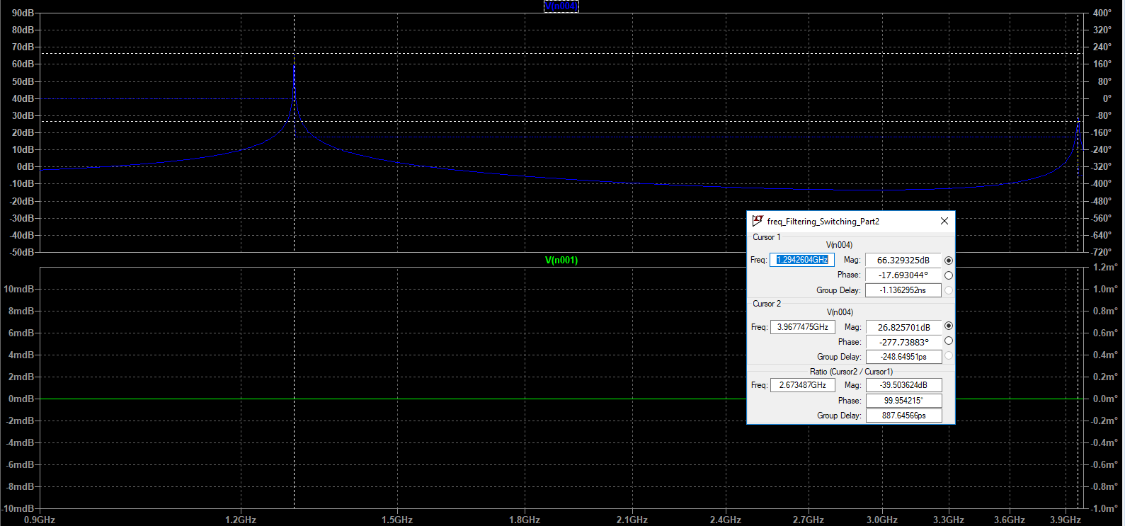
As attached, I did a simulation on LTspice running from 1MHz to 4 GHz. I ran it through a filter and was expected to see if the circuitry allowed me to attain the best reading of my values at 3.2GHz. Is it possible to say then that the peaks, corresponding to the resonant frequency attained form the circuit, are a result of a bandpass filter and that this means that the value attained shows that the circuit is not optimised for said frequency?

If not, how would i interpret these results.

(background info, these (1 of many)
advice on schematic.PNG
graph output.PNG
are outputs from a synthesizer board)

Thank you in advance!

additionally i realised i may have used the wrong terminology, not resonant but cut-off freq!
 
Last edited:
something fishy with your filter. Does the source have a finite source impedance like 50 Ohms? Is the filter terminated with a load impedance? Why are C5 and C6 in parallel? Why are none of the nodes labeled?
 
something fishy with your filter. Does the source have a finite source impedance like 50 Ohms? Is the filter terminated with a load impedance? Why are C5 and C6 in parallel? Why are none of the nodes labeled?
ahhh my bad. i accidentally mislooked my schematic and it came out funny. I'll update the new schematic for anyone who is stiil willing to help..
advice 2.PNG
 
Questions to ask when designing a filter:

What is the source (impedance)?
What is the load (impedance)?
What (frequencies) do you want to pass? How much insertion loss can you tolerate?
What (frequencies) do you want to block? How much attenuation?
 
Why C7,8,9,10 and R1,2,3?
Hi man! thanks for the reply! actually its a 3.3V voltage connected to an output from a synthesizer( supposedly outputing 4 frequency levels so R1,R2,R3 are supposedly inputs to that part of the circuit (for the other frequency levels). I decided to implement them separately to kind of simplify it for my mentor/explanation purpose to view my project.
Sadly, the schematic is confidential and i cannot share it here. :(

Questions to ask when designing a filter:

What is the source (impedance)?
What is the load (impedance)?
What (frequencies) do you want to pass? How much insertion loss can you tolerate?
What (frequencies) do you want to block? How much attenuation?
Additionally, the much information that i have from this circuit is just that it's a synthesizer board meant to generate an LO signal as well as frequencies at 4 different levels (one of which is 3.2GHz as shown here).

the only thing i can do (or did) was to calculate cut-off freuency and i have discussed it with mentor about the capacitor values being low and in a real life setting (based on tolerances) the freq band may drift quite a bit.

I am still unsure if i am missing out anything in my analysis and again i am lost as the only information left for me was teh schematic without much direction but to simulate .

Thank you guys again for your time!
 
Status
Not open for further replies.

Latest threads

New Articles From Microcontroller Tips

Back
Top