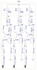
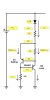
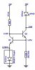
This configuration of two PNP transistors create a negative feedback to each other keeping the currents and voltages in-check. Both transistors come to a rapid equilibrium.
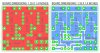
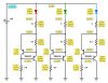
Circuit Simulation and Calculations (Please see attached diagram):
Known: In this configuration Setting Transistor (Q1) is driven in "Just ON" while Load Transistor (Q2) is driven in "Saturation" modes.
Datasheet for Q1 & Q2: 2N4403 TO-92 Package, Ic(max)=600ma, Vbe(on)=0.65v, Vbe(sat)=0.75, Vce(sat)=0.85, Pd=625mw
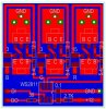
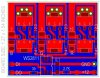
Datasheet for WS2811: Constant Current Output (Sink) at 18.5ma
Datasheet for HP RGB 10W: Vf(red)=6v, Vf(grn)=9.6v, Vf(blu)=9.6v, I-led (max)=350ma (We are driving the LED's at 300ma, Vcc=12v)
Evaluation: Since Q1 is driven at ON status then its Vbe=0.65v, Q2 is driven at Saturation then its Vbe=0.75v and Vce=0.85v (min)
1- Since Vce2=0.85v and Vbe=0.75v then V1=0.85-0.75=0.1v. We also know Iws=18.5ma hence Rws=0.1/0.0185= 5.4 ohms
2- Since Vce2=0.85v then V2=Vce2=0.85v
3- Since Q1 is in On status, Vbe1=0.65v. Therefore V3=V2+Vbe1=0.85+0.65=1.5v
4- Vx(red)=Vcc-Vf(red)-V3=12-6-1.5= 4.5v, we also know Vx=Rx * I-led therefore Rx=4.5/0.3= 15 Ohms
5- Vx(grn)=Vcc-9.6-1.5= 0.9v then Rx=0.9/0.3= 3 Ohms
6- Vx(blu)=Vcc-9.6-1.5= 0.9v then similarly Rx= 0.9/0.3= 3 Ohms
7- Looking up the datasheet of 2N4403 we note that Ib1(on)= 1.5ma and at this current hfe1=10.3= Ic1/Ib1 then Ic1= 15.5ma and Ie1= 17ma, Is= 283ma
Approx.: Ie1=0.057 x (I-led) and Is= 0.943 x (I-led), (I-led)=Ie1+Is
8- Vs=Voltage across setting resistor, Vbe1=0.65=Is*Rs. Rs=0.65/0.283= 2.3 Ohms
9- Power Dissipation Calculation:
Pq1=Vce1*Ie1=1.4x.017= 23.8mw, Pq2=Vce2*Ie2=0.85x(0.283+.0015)= 242mw, Prs=Vs*Is=0.65x0.283= 184mw
Prws=V1*Iws=0.1x0.0185= 2mw, Prx(red)= Vrx*(I-led)= 4.5x0.3= 1.35W, Prx(grn)=Prx(blu)= 0.9x0.3= 270mw. Recommended Power Rating for Rx(red)=2W, Rx(grn)=Rx(blu)= 0.5W