R-led; LEDs are not like resistors at all. They are Zener diodes.
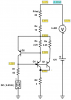
Resistor; When the current is cut in half the voltage drop is also 1/2.
LED; A 2:1 change in current results in about 5% change in voltage. (depends on part)

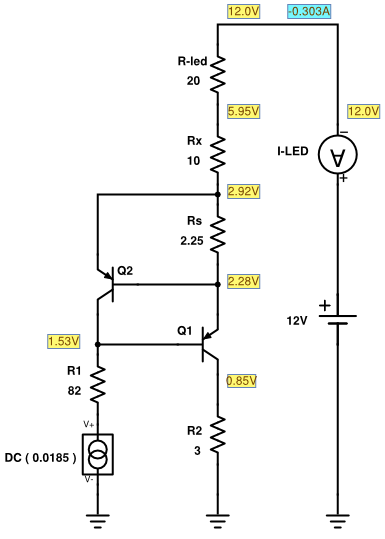
R2 reduces heat in Q1. Good but reduces the ability to pull down if the voltage is low.
R1 reduces the ability to pull down when the voltage is low.
DC(0.018) current source. In LT-Spice the current sources will pull negative. This fooled me at first. The voltage between the current source and R1 when to -2 volts. This is not real life. It make the circuit look like it would work at lower power supply voltage. Watch out!
Resistor; When the current is cut in half the voltage drop is also 1/2.
LED; A 2:1 change in current results in about 5% change in voltage. (depends on part)
R2 reduces heat in Q1. Good but reduces the ability to pull down if the voltage is low.
R1 reduces the ability to pull down when the voltage is low.
DC(0.018) current source. In LT-Spice the current sources will pull negative. This fooled me at first. The voltage between the current source and R1 when to -2 volts. This is not real life. It make the circuit look like it would work at lower power supply voltage. Watch out!