Continue to Site

Welcome to our site!

Electro Tech is an online community (with over 170,000 members) who enjoy talking about and building electronic circuits, projects and gadgets. To participate you need to register. Registration is free. Click here to register now.

  • Welcome to our site! Electro Tech is an online community (with over 170,000 members) who enjoy talking about and building electronic circuits, projects and gadgets. To participate you need to register. Registration is free. Click here to register now.

Solid State Tesla Coil Burning Mosfets

Status
Not open for further replies.

Nissan20det

Member
I have a full bridge setup I just made, I have ran it on a couple small power supplies. 20v 90W laptop charger, 28v 2a transformer. It works quite well. Now I don't have a variac to step up mains slowly(USA 120vac). What I came up with was a CFL LED 150watt dimmer. I first just tested its output voltage after rectifying and using a light bulb for load. I got it down to 18v Sweet!!! So I went ahead and tested it. First try, I got light up right away . Of course me being to excited I started to turn it up and up. Totally spaced I had a 120watt halogen for load...oops... I meant to lower the crap out of that once I established my first light. So It fried the dimmer along with two Mosfets(1 High and low side)...

Well I fixed that, So second try... I get it to light up but only for 5-6 seconds and it dies, dimmer starts to hum. I Look all through my circuit and realized when I changed my lower current fast switching diodes for higher current ones I plugged one of the diodes and drain output one bread board pin off(I did this before the first test) So My first light was on a screwed up half bridge. Plugged that in correctly, replaced the Mosfets on the other sides high and low side. So third try, This time still with 120w bulb just to start, I turn it on and wow way better then the first light, probably 4 inch streamers with dimmer all the way down.(Full bridge definitely working now) I shut it off and try a forth time, Lights up again... Sweet!!! so before anything else happens i turn it off grab my phone for video, set it up, turn it on ....nothing, I also hear a hum. Its the dimmer, popped a high and low side Fet again!!!!

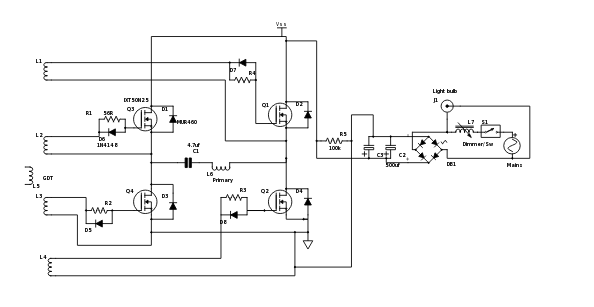
Here is my H bridge setup
sstc (4).png


Then I did add two 15v zeners in series, anode to anode, gate to source. blew another two mosfets... UGHH.... I should have my freewheeling current covered with my MUR460's, voltage spikes with zeners, and dead time with 56ohm and 1n4148 on gate. Im so lost any help would be great. Ill check what my actual dead time is on my scope tomorrow. The only thing I can think of is the tesla coil is about 4ft from the driver circuit on the same table, maybe the output from TC is affecting the Gate Drive Transformer through RF? Maybe causing it to turn the other "OFF" fet ON. ahhhh Im so lost!!!!

I do see now that Its always a high side and low side that pop. but ones that are turn on opposite of each other. So say always the high and low on the same side of primary(oppositely switching). So it makes since that I am turning one ON as the other isnt fully OFF. Now with my dead time theoretically being tackled, thats why I lean towards interference. This is also on a bread board, Maybe H bridge impedance is to high, I could double up all my jumpers.. What do you guys think?

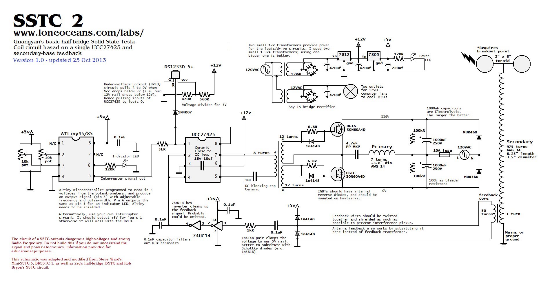
To help you understand my driver circuit, here is another schematic, Im using his fet driver but to a 4 fet GDT. and the modulator is a multi vibrator in my situation. Overvolt protection on driver circuit is not used and his feedback transformer i could not get working. so I am using a antenna in its place. The H bridge Is the other pic. Thanks in advance guys!!!
LoneOceans SSTC.jpg
 
Why not build a conventional Tesla Coil it is 100 times easier and works 100 times better.

**broken link removed**

**broken link removed**

**broken link removed**

**broken link removed**
 
My guess is that your issue is twofold:
  • Your interrupter has too high of a pulse width. You should aim for a <10% duty cycle
  • You're using MOSFETs. There is a reason Guangyan used IGBTs in his design. At the high currents seen in a Tesla coil H-bridge, the MOSFET acts as a resistor, and the power dissipated is P = I^2 * R. IGBTs have a fixed voltage drop, however, so the power dissipation is only P = I * V. When using FETs, the power dissipation increases exponentially with current, whereas with IGBTs the power dissipation only increases linearly with current. IGBTs are far more efficient in Tesla coil circuits, and are less susceptible to overheating due to high power dissipation.
Speaking of overheating, what have you got for a heatsink and cooling fans? Can we see photos of your setup?

He's over at AAC too, if you look at the O/P, he says this, "I plugged one of the diodes and drain output one bread board pin off". And from what he showed over there he's telling it like it is.
 
Yes i did pin it wrong one time. it also ran the longest when that pin was off, lol. but that was a wile ago and was fixed right away. I have already made a SGTC, I wanted to challenge myself, the SGTC was super easy.

Now on IGBT's I did not know that. Now I did get IGBT's for this project. I got 4 IRGP50B60PD1. But I figured I have alot of mosfets and only 4 IGBT's So If its blowing fets I figure I'd be blowing those too. Now I am not overheating one bit. these just stop working, no signs of damage they just stop working. So that does make since on what ur saying, but I think is that where the case I would see some heat. I mean the are not even warm.

I have very good heat sinks

It's not so much external heating that kills the MOSFETs as it is the internal junction temperatures. That's what comes from high power dissipation.

The other possibility is that you're getting inductive voltage spikes on the MOSFETs due to improper flyback diodes. If the diodes shown in your schematic across the drain and source of the MOSFETs are built-in to the device, it will not be sufficient. They tend to be way too slow and will not protect against lots of the transients. This could potentially be a cause for MOSFET damage.

My recommendation would be to buy lots more IGBTs, and make sure they're fast. Slow IGBTs will also fail as they will try to turn off too late when there is significant current flowing through them.

Did you watch the bridge switching waveforms with a scope to make sure you don't need phase lead?
 
The point I was trying to make was your building this on a breadboard. Not a good thing to do for something like this project. At a minimum it should be soldered on a generic type proto board.
 
Once completed this will go on a proper photo etched board. I want a working circuit before soldering. Hard enough to unmount and rsmount these MOSFETs 8 times, let alone soldering.

Ya I guess I can see them internally heat up. As long as that can happen in a millisecond. Also the MOSFETs I'm using have internal bridge diodes, altho I am not relying on those, the ones in schematic are MUR460's 4amp 24nano second ultra fast switching diodes. I got those of that other guys circuit. Alot of coilers use these MUR series.

I have scoped everything, all looks great. But phase lead? Not sure what that is, Could you explain that to me. I thought I had a Driver issue today but I was just being dumb. But ya scope pics look good.

I have a problem trying to test dead time. I have a miniDS202 2 channel 1mhz scope. I am trying to look at the input signal on a high and low side fet at the same time. Problem is if I ground the scope to (high voltage) Hbridge side ground, I can read the low side gate signal just fine since the other gdt legs are grounded on low side fet source. Now if I put my other probe on the high side gates it read super high voltage. This is because my scope isn't seeing the source side of the high side fets as ground. So is there a way to make a floating or theoretical ground from the high side fets "source" and low side fets "source"? Only way I could come up with is changing the probe on the high side gate to x10 and dropping voltage on scope from 10-1v that kinda works but I can see the waveform has a hump at the end that isn't normally there is I ground on the high side source like normal. But if I do that then the low side fets gate has that hump..
 
Can you please post a screenshot or photo of your bridge switching waveform (not of the MOSFET G-S waveform, but the actual output of the bridge? "It looks great" is hardly a quantitative observation :p

When probing the G-S waveform you should not see a high voltage. The only way you'd see that is if you were attaching the ground lead of the scope to the ground of the H-bridge, which is not the correct way to do this. You need to attach the ground lead of the scope probe to the source of the MOSFET under test, and probe the gate. Be careful when doing this though -- you MUST put your scope on an isolation transformer. The ground lead of the oscilloscope is connected internally to mains neutral. If you put the ground lead on the source of a high-side FET, you're shorting the bridge output directly to the neutral line, which will likely destroy your oscilloscope.
 
Once completed this will go on a proper photo etched board. I want a working circuit before soldering. Hard enough to unmount and rsmount these MOSFETs 8 times, let alone soldering.

I understand that but breadboards aren't meant for this type of circuit. Even 'dead bug' or 'manhattan' building styles are better for this than a breadboard. Or even wire wrap.

Limit's of breadboards. http://dangerousprototypes.com/blog/2011/12/05/breadboard-limitations/

Dead bug and manhattan style. http://hackaday.com/2016/05/04/getting-ugly-dead-bugs-and-going-to-manhattan/

Wire wrap. http://makezine.com/2009/07/27/lost-knowledge-wire-wrapping/
 
Shortbus is correct, using a breadboard for this type of circuit will severely limit its capabilities, will affect the parasitic inductance and capacitance of the design, and will cause it to function differently than it would in a PCB. Additionally, breadboards are not capable of handling these voltages and currents, and you will likely severely damage your breadboard if you continue to use it.
 
Ya that's fine if it breaks, I have h bridge double jumpered to help impedance. Also I just what it to work on this then it will be transferred. I'm talking very short periods. I haven't came close to running the full potential of mains through this pcb. Do u really think I'm instantly popping mosfets due to the bread board? Honestly if I could get this to run like I did the first try. Constant on and off switching with a couple min runtime. I would go ahead and go right to my photo board. I can make the photo board now. I would just hate to have to re design it if something is wrong. It takes a good amount of time.

On the scope part. Yes I will post my h bridge output today. And when I said I connect the ground of my scope to the ground of the h bridge. That is connecting it to source. The two low side fets source's are connected to ground. The two high side fets source is connected to the primary (OUTPUT). My scope is portable, and is not connected to mains internally. DS202 is the model. The problem I'm having is to see my GDT Waveform correctly I need to ground on one output and probe the other on each separate coil. Now the low sides are tide together at ground (low side fet source). High side GDT's outputs connect to gate and source of the high side fets. So I can't see a high and low gate waveform at the same time. I want to so I can see my dead time. I some how need to ground my scope on the low side fets source (ground) and the high side fets source (primary out) without shorting it.

Could I use two caps in series from high source to low source and ground the scope in the middle of the two caps?
 
Last edited:
I think you're missing the point. Using a breadboard for this sort of project is going to affect its operation and the results will be unreliable. We're not just saying you shouldn't be using a breadboard, we're saying you can't use a breadboard. It just won't work correctly.

Forget about the gate-source waveforms for now, instead look at the output waveform of the H-bridge. That will give you all the information you need to know (at this point, anyway).
 
Okay will do I'll make my photo board today and post some scope pics as well. I'll post it's output open and under primary load. Should I ground scope to one side of h bridge and probe the other?
 
No, you will need to do a differential measurement. Additionally, if you want to continue with this project you really need an actual scope. One of those crappy little USB ones will not do the business.
 
I beg to differ, this is a name brand ds202 not a knock off.. but we had this along side with a tektronix 3012 I had at my old job and it was quite on. I will say it's been 2 years since that comparison we did and I noticed my waveforms wiggling a little but I 100% trust my scope lol. I did my research and my own testing. And I'll never go table top lol. No offense. I may eventually get a keysight portable. But I love the ability to move it where u go not the other way around.

By differential do you mean ground scope to ground. have one probe on one output and the other probe on the other? And to a subtraction?
 
Do not connect the scope grounds. Probe the two sides and do an A-B operation.

And trust me, no portable USB scope, whether name brand or otherwise, will be able to do the job that a real benchtop scope can. Especially for this sort of project.
 
Well tried to do what you said. My scope is acting like the voltages are super high since I don't have it grounded. It can't see the bottom so it off the charts. Even on x10

Any other ideas?
 
Well it works if I don't have the primary connected. So unloaded. I get this pic7 is 10v 10v 2us pic 9 is 10v 10v 1us

I did notice how channel 2 (Yellow) Is slightly larger than the blue channel 1. I thought maybe the GDT output is making one side of the fets open more??Maybe more voltage at gate? So I swapped just the low side with the other low, then high with high, then both. I still get a larger voltage on channel 2. Maybe in the 2 years I have used this chan 2 has been used 10% of that of 1. I also thought DC blocking cap since thats on chan 2.. I then swapped on which side of the primary output chan 1 and chan 2 are. so now on opposite sides chan 2 is still larger. So thats gatta be the scope. lol Theirs ur lecture about scopes coming to play lmao hahaha...


Edit: Scratch that I am using two different probes from two manufacturers, One is a switchable x1-x10 probe the other is the factory probe only x1. That is my problem ur seeing. I swapped chan 2 probe with chan 1 now chan 1 is high. so 100% for sure the higher voltage seen is the 2 different probes., my x1-x10 probe reads a little lower voltage... First time I have seen that. I will absolutely get another factory and x1-x10 so I can match probes resistance. one probe is 324ohms the other is 1.2ohms. I am sory for that effect I know that throws off the subtraction. I will try to match resistance with resistors to see if that helps....
 

Attachments

  • img_009.bmp
    38 KB · Views: 142
  • img_007.bmp
    38 KB · Views: 130
Last edited:
here is the hbridge under load. I did get it to work.. but of course Im sory for the different probe inputs I know that may make this useless. This is also with inverter out of phase. that was the only way to see it.. with it in phase its off the grid like I said..

Is it the hump on the blue thats causing my issues? maybe thats not there when I am in phase? I did try switching every part from side to side including GDT connections and I could not get the hump to switch to the othere side of primary(other channel). But if I switch the probes around it does switch, so it is always on one side of primary, altho moving parts around didnt.
 

Attachments

  • img_011.bmp
    38 KB · Views: 141
Last edited:
Status
Not open for further replies.

Latest threads

New Articles From Microcontroller Tips

Back
Top