Continue to Site

Welcome to our site!

Electro Tech is an online community (with over 170,000 members) who enjoy talking about and building electronic circuits, projects and gadgets. To participate you need to register. Registration is free. Click here to register now.

  • Welcome to our site! Electro Tech is an online community (with over 170,000 members) who enjoy talking about and building electronic circuits, projects and gadgets. To participate you need to register. Registration is free. Click here to register now.

Simple load cell circuit with Ins Amp output to arduino.

Status
Not open for further replies.
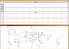
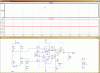
The working schematic is wrong, it's very tightly put together so it's hard for me to see where do the legs go, i'm inspecting the circuit closely again to draw more accurate schematic.

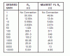
Resistors on Vin+ are 10K ohm one (set to 5,5K) and a 33K ohm.

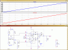
I'll check the voltage on monday, i don't have the access to the load cell at the moment.
The original schematic is wired exactly as shown.
 
Ok, i've corrected the schematic, and i found out that i've falsely wired the schematic. With this circuit:
Navor Copy.png
i'm finally able to get proper readings from load cell. But now i have a different problem, the 106 tantalum capacitor that goes between pins 2 and 4 on the 7660 starts to smell after a while and has already changed colour to a bit darker tone.

I don't want the circuit to fail soon so i'm thinking of replacing the 7660 part of circuit with 2 diodes, is this still possibile, and what would the circuit look like?
 
Ok, thanks, will a 10uF 25V electrolytic cap be ok?

How can i check for ESR, and what would be low enough?
 
I use the 7660 all day... They are charge pump caps so as long as they AREN'T tants they be okay... +5v to -5v is 10v so 16v+ will be okay... I use cheap electrolytic caps as I only use tiny a current...
 
Thanks for all your help, i was able to finish the circuit and it worked... till the arduino failed... less than 3 months of very light use...
do you think this circuit is too much for arduino to handle (arduino is powered by USB port)

i've read that max reccomended current for output pin on arduino is 20mA,
max safe current is 40mA, do you thik this circuit pulls more than that?

The arduino was a cheap china model, so it could be just the bad quality tho, just want to be sure that the next one wont follow that fast too...
 
You need to post a schematic of how the load cell circuit is connected to the Arduino. You also need to specify HOW the Arduino has failed.

Les.
 
Same schematic as in post #22, the gnd is from arduino and instead of 12v it's the 5v that arduino supplies and out is connected to analog0 pin...

Just failed, leds turn on when it has power, but is not recognized by any pc using both Windows & Linux
 
hi,
Your circuit in #22 is incorrect.
The load cell excitation should not be connected to the IA amp input, but to the 5V/0V supply.
The L/C output common mode voltage at the IA input should be ~2.5v.

The 10K pot and 33k resistor are a simple way of nulling a L/C offset, in one sense only.

As the IA is powered by +/-5V , it is possible that the IA output to the Arduino could swing negative. This could bias the clamp diode in the MCU to be biased 'hard on' which could damage the ADC input clamp,

Without any load on the cell, what voltage do you measure at the IA output pin ? [ do not have the MCU ADC input pin connected ]

E

BTW: with a 10R on the gain pins the gain is ~5000.!!!
 

Attachments

  • AAesp01.gif
    AAesp01.gif
    11.5 KB · Views: 183
If the Arduino board is not seen by your PC then the chip that does the USB to serial conversion faulty. This may be an FDTI chip of it could be another ATmega chip used as a USB to serial converter. On the Arduino Uno that I have (With the DIL ATmega328P) they use an ATmega16U2 for this purpose.

Les.
 
hi,
Your circuit in #22 is incorrect.
The load cell excitation should not be connected to the IA amp input, but to the 5V/0V supply.
The L/C output common mode voltage at the IA input should be ~2.5v.

The 10K pot and 33k resistor are a simple way of nulling a L/C offset, in one sense only.

As the IA is powered by +/-5V , it is possible that the IA output to the Arduino could swing negative. This could bias the clamp diode in the MCU to be biased 'hard on' which could damage the ADC input clamp,

Without any load on the cell, what voltage do you measure at the IA output pin ? [ do not have the MCU ADC input pin connected ]

E

BTW: with a 10R on the gain pins the gain is ~5000.!!!

What do you mean, it is connected to the 5V and GND...
I haven't checked that but if i remember correctly it was somewhere in the 2.5V range...

What do you mean with nulling L/C offset in one sense only?

The IA output is always 2.90V - 3.10V now no matter if the load cell is pluged in and stressed or not.

the Load cell i'm using has 120ohm bridge, so i need to use 10ohm gain on IA to get decent values.


I'm thinking of just using HX711 to do the the work instead of this circuit, and it's cheaper than all of the elements i've used...
 
If the Arduino board is not seen by your PC then the chip that does the USB to serial conversion faulty. This may be an FDTI chip of it could be another ATmega chip used as a USB to serial converter. On the Arduino Uno that I have (With the DIL ATmega328P) they use an ATmega16U2 for this purpose.

Les.

It was a chinese arduino that has CH340T in place of MEGA16U2, but uses the same ATMEGA328P... it's a 5 bucks board that i don't wanna waste time fixing, was just curious if it could be caused by the arduino...
 
What do you mean, it is connected to the 5V and GND...
Your diagram clearly shows the excitation points of the bridge connected to the input of the amplifier, the excitation of a bridge should be connected to the supply voltage

I haven't checked that but if i remember correctly it was somewhere in the 2.5V range...
Being 'somewhere' in the 2.5V range, with a bridge is not accurate enough.

What do you mean with nulling L/C offset in one sense only?
As the 'variable resistance is connected to only one input of the IA, means its only across one arm of the bridge. which means you can only reduce the effective resistance of that bridge arm.

The IA output is always 2.90V - 3.10V now no matter if the load cell is pluged in and stressed or not.
The output of the IA, with Vref connected to 0V, if the bridge is correctly balanced, without any load, should be close to zero volts.

the Load cell i'm using has 120ohm bridge, so i need to use 10ohm gain on IA to get decent values.
The value of the bridge arms [elements] has no effect upon the gain setting.

Hi,
If the output of the IA is at ~3V then your bridge or IA is incorrectly wired ,the bridge or IA is faulty.

If you have a millivolt meter , measure the IA input, across the bridge input pins, it should be close to zero
E
 
hi,
This is a LTSpice sim of your circuit, I have modelled the 1NA114 [ its inside the dotted box]

Figure #1:
With the 33k and 5k5 Pot connected the inputs signal is -3.9mV which drives the IA into negative saturation at ~ -4.8V.

Figure #2:
With the 33k and 5k5 disconnected the IA output is zero volts, which it should be.

Figure #3:
With V3 source simulating a 1mV input signal, even at 1mV input the IA is driven into saturation.

Reduce the Gain and remove the 33K/5k5 and remeasure Vout.

TIP: keep the bridge connected to the IA input, then add a shorting wire across the IA input pins, the IA output should be close to zero volts.

E
 

Attachments

  • Fig1.gif
    Fig1.gif
    39.1 KB · Views: 157
  • Fig2.gif
    Fig2.gif
    35.8 KB · Views: 170
  • Fig3.gif
    Fig3.gif
    39.3 KB · Views: 176
Status
Not open for further replies.

Latest threads

New Articles From Microcontroller Tips

Back
Top