Continue to Site

Welcome to our site!

Electro Tech is an online community (with over 170,000 members) who enjoy talking about and building electronic circuits, projects and gadgets. To participate you need to register. Registration is free. Click here to register now.

  • Welcome to our site! Electro Tech is an online community (with over 170,000 members) who enjoy talking about and building electronic circuits, projects and gadgets. To participate you need to register. Registration is free. Click here to register now.

RF signal amplification

Status
Not open for further replies.
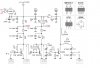
is anybody going to help? i'm not RF expert... i said i'll try to do my own design and then i'll upload it here so we can comment it and i learn something from it..

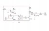
the two 10-30pF variables caps exist so i can match the impedance between stange depending the frequency... probably the values i'm using aren't correct?
 
I'll ask again, do you understand that the two trimmer capacitors are in parallel?
 
You still don't seem to understand my reasoning.

At RF the capacitors are in parallel because the battery (which should have a decoupling capacitor) is a low impedance to RF so both supply rails are both 0V as far as RF is concerned.

As I said above, with C3 and C4 connected as per your schematic, the total effective is equal to the sum of their values.
 
That's a but harsh Nigel, go easy on the nube!

He did ask! :p

C4 and C3 are effectively in parallel with each other giving you 20pF to 60pF; are you aware of that?

I'm fully aware of that, but why would you connect two trimmers like that? - you wouldn't, unless you've drawn it completely wrong. They should form a potential divider from one stage to the next, as discussed previously, to match impedances.

Have you tried simulating it?

I don't do simulators.
 
I'm fully aware of that, but why would you connect two trimmers like that? - you wouldn't, unless you've drawn it completely wrong.
That's what I'm asking him.


I don't do simulators.
Pehaps you should learn to simulate.:p
 
Perhaps, Wiz115 meant that C3 as parallel to L2 and C4 as feed back cap for oscillation. But he shifted the emitter resistor to collector and decoupled it. The oscillator is thus a failure.

Next error appears inductor linkage of U1 collector to U2 base, that would pull down the U1 collector voltage to 0.7V approx.
 
Last edited:
I thought this was supposed to be an amplifier, not an oscillator, although it is easy to acidentally build an oscillator.:D
 
why not build it like it is in the data sheet? just double the cap and inductor values which will make it work at 1/4 the original freq of 400Mhz = 100 Mhz... you don't have to re-invent the wheel..... once you get it in the ballpark, then you can tweak it.

fairchild has SPICE models for these transistors most likely. go to:
Fairchild Semiconductor - Models and Simulation Tools

you will have to fill out a form and they email the models to you as text files. either the HSPICE or Pspice 3 models should work
 
hi!

check the new schematic..i believe i corrected it, it wasn't to my intentions to connect the variables caps like that... i was careless when drawing the schematic and afterwards i didn't noticed it since you highlighted it.

any other problems with my design?


P.S hero999 i thought you asked me about simulation and the rest...then nigel responds like if your question was going to him... you asked me or him or both of us? :D


why not build it like it is in the data sheet? just double the cap and inductor values which will make it work at 1/4 the original freq of 400Mhz = 100 Mhz... you don't have to re-invent the wheel....

well said...

but then again doing what i'm doing also helps me learn how to think and make a design :)

notice the mistake with the variable caps...it was because i was careless when drawing.

let's go on now... :)
 

Attachments

  • rfamp2.jpg
    rfamp2.jpg
    20 KB · Views: 741
Last edited:
Hi Whiz,
Your circuit is missing a very important supply bypass capacitor.
 
1) (repeat of ag) Battery should be bypassed.

2) R1 is good for HFE at minimum, but what is the bias point for HFE at maximum? With no max HFE specified for BF199, I would use a bypassed emitter resistor and a fixed base bias point, but that's just me. Do you intend class A or B?

3) With a little calculation, you should be able to determine a fixed value for C3. What do you expect will be your nominal setting for C4?

4) There is no base bias on U2. It won't ever conduct.

5) R3 should be bypassed unless you really want it to soak up your RF and lower your output Q.

6) What are the values and characteristics of L2 and L3?

7) I would like to see the typical reactance (R, +j, -j) that you expect, at the operating frequency, in the output pi filter so I don't have to re-do your math. You did do the math,, correct?
 
Last edited:
Where is the original RF amplifier project that Whiz copied wrong?
It has the capacitive voltage divider and has the 2N3866 biased in class-C without any bias voltage.
 
Last edited:
You don't need a bias voltage on the 2N3866, but you do need a return path for the base current, especially in class C. The base itself only conducts one way.
 
Last edited:
the one in post 2 looks like this...... the transistor is running class C, but with the filtering shown, the output signal must be rich in harmonics....
 

Attachments

  • rfamp2.jpg
    rfamp2.jpg
    69.1 KB · Views: 370
P.S hero999 i thought you asked me about simulation and the rest...then nigel responds like if your question was going to him... you asked me or him or both of us? :D
I was asking you.
notice the mistake with the variable caps...it was because i was careless when drawing.

let's go on now... :)
So it was a mistake, I didn't know if it was intentional; that's why I was asking you.
 
Hi Whiz,
Your circuit is missing a very important supply bypass capacitor.

i'll add it later when i'm going to update my schematic, thanks!


1) (repeat of ag) Battery should be bypassed.

2) R1 is good for HFE at minimum, but what is the bias point for HFE at maximum? With no max HFE specified for BF199, I would use a bypassed emitter resistor and a fixed base bias point, but that's just me. Do you intend class A or B?

the BF199 on my circuit works on class A since my design is theoritical and i haven't checked the hFE of the transistor i believe this is a good way to go.

3) With a little calculation, you should be able to determine a fixed value for C3. What do you expect will be your nominal setting for C4?

i don't know what i should expect for that i still haven't understood the concept behind it...i only know it forms a capacitive voltage devider and you can regulate the impedance so you don't drain the previous stage..

are you willing to help me understand it? and also do the maths for a fixed value?!

4) There is no base bias on U2. It won't ever conduct.

my coil filters out the signal right? i didn't noticed that too... since i had in mind to make the impedance match circuit between stages.

5) R3 should be bypassed unless you really want it to soak up your RF and lower your output Q.

i thought only preamplifing stages need that much decoupling so i'm
only using a choke...


6) What are the values and characteristics of L2 and L3?

it's

2 1/2 Turns
Impedance: 50 MHz • 800ohm
Impedance: 100 MHz • 550ohm

check the photo...

7) I would like to see the typical reactance (R, +j, -j) that you expect, at the operating frequency, in the output pi filter so I don't have to re-do your math. You did do the math,, correct?

haha! now you got me... :D it's not that well calculated since i had a bit of a problem with the link barcbarker gave in past pages... it says 500MHz and i don't know how to remove that value so i can calculate mine.
 

Attachments

  • chokeh.gif
    chokeh.gif
    6.4 KB · Views: 251
Last edited:
Status
Not open for further replies.

Latest threads

New Articles From Microcontroller Tips

Back
Top