Hello Everyone,
I am new here and found this place serendipidously online looking for circuit diagrams/info/etc. I have picked this circuit to try to hone my circuit development skills, maybe this will help others as well.
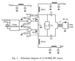
This is an RF power supply, I think I have figured out the front end which is using d flip flops with a crystal oscillator to create the initial 13.56 MHz digital signal (this is where I was thinking of using an fpga with a crystal modified clock input) which is fed to a pair of amplifiers (I’m guessing these are power op amps) which is more or less a giant amplification chain to get to the mosfet gate which acts as an oscillator for a high power AC source?
So some confusion arises for me, are the 2 Vdd just the AC terminals (at 60 hz?) , I would think these would have to be DC other wise you would get some wierd convolution when you applied gate signals to the mosfet with AC across it? Also what is the purpose of the 2 capacitors to ground with an iron inductor between, are those just noise filters? What would happen if rfc1 and 2 were removed? So the tank circuit acts as a filter (assumed to be tuned to 13.56) to make sure only that frequency passes, what are C1 and C2 for? I might try my hand at doing the LC and C1 C2 voltage calc in time domain, freq is easier but have you ever found yourself in a situation where you finish the loop calc and can’t take the inverse Fourier transform?

I picked this as I would eventually like to build an RF sputter machine (since my understanding is that an RF sputter can do non metalics such as DLC coatings etc.
MicroSemi
IEEE
I am new here and found this place serendipidously online looking for circuit diagrams/info/etc. I have picked this circuit to try to hone my circuit development skills, maybe this will help others as well.
This is an RF power supply, I think I have figured out the front end which is using d flip flops with a crystal oscillator to create the initial 13.56 MHz digital signal (this is where I was thinking of using an fpga with a crystal modified clock input) which is fed to a pair of amplifiers (I’m guessing these are power op amps) which is more or less a giant amplification chain to get to the mosfet gate which acts as an oscillator for a high power AC source?
So some confusion arises for me, are the 2 Vdd just the AC terminals (at 60 hz?) , I would think these would have to be DC other wise you would get some wierd convolution when you applied gate signals to the mosfet with AC across it? Also what is the purpose of the 2 capacitors to ground with an iron inductor between, are those just noise filters? What would happen if rfc1 and 2 were removed? So the tank circuit acts as a filter (assumed to be tuned to 13.56) to make sure only that frequency passes, what are C1 and C2 for? I might try my hand at doing the LC and C1 C2 voltage calc in time domain, freq is easier but have you ever found yourself in a situation where you finish the loop calc and can’t take the inverse Fourier transform?
I picked this as I would eventually like to build an RF sputter machine (since my understanding is that an RF sputter can do non metalics such as DLC coatings etc.
MicroSemi
IEEE
| ReplyForward |


