Hi
I am having the following problems with EasyEDA.....the user interface just doesnt seem to have the controls needed.
Can anyone shine light here?
I am an eagle pro user and could use eagle pro as soon as i bought it...but this company insists on easyEDA.
Eagle Pro problems can be solved by googling them or asking on forums...not so easyEDA
PROBLEMS WITH EASYEDA
**…Cant save partially finished footprints without it moving them about. (centralizing them)
**..Creating custom schem symbol…how to copy from pre-existing one?
**..Moving a pin in symbol editor…it moves the number instead.
**..How to make a particular component library file…eg , for a particular board.
**..How to delate a branch of a net in the schem editor…without deleting the entire net?
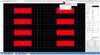
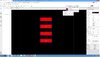
**..Copying a line of pads to a different, particular place…eg when making a square, 32 pin micro (8 pads per side).
**..In schem editor, the symbols can be moved off the net wires, without the net wires being connected to them.
**..Wouldnt let me make a custom component called resistor because it said one such named already existed…..but I wanted to create it in a particular library so a “same name” should be allowed?
**..How to do “zoom to selection” in schem editor?
**..Nets not connected but look connected (they separate when the net is moved). In Eagle you simply “dot” the joint and they get joined…how to do this in easyEDA?
**..How to “Highlight net” in schem editor?
**..In schem editor, when you click on a net, it doesn’t tell you what that net is?
**..How do you show the “GND” net in the schematic editor?
**..What is the name of the net that the provided GND symbol gives you…how do you find this out?. There doesn’t seem to be a “supply” pin that you can select in the schem symbol editor?
**..How can I pick a symbol in the schematic editor and click to edit that symbol, straight from the schematic editor.
**..The different resistors in the schem editor may sometimes have the same footprint…but not the same value….how can I input a value to a resistor symbol in the schem editor. I hope I don’t have to make a different resistor symbol for each different resistor value?
**..How do you make a library called “Control_PCB”, and put components into it? Certain PCBs have certain components in them…and the easiest way to find these again at a later date, is to remember which PCB they are on..then go to the library of that PCB name….rather than having to accurately remember a long part number.
**..The EasyEDA GND symbol has three variants…..but they look exactly the same….how do I know if my ground is the same in my schematic if I cant click on it and interrogate its exact name, or highlight it?
**..I have two grounds in this schem. Its got isolation. I wish to make a different ground symbol for each ground. How do I make it so that whatever I connect to each, gets called the name of that ground?
**..In schem editor, how do you do “move selection”?
**..I just picked an 0603 resistor out of the LCSC electronics library…and when I checked it, it said it was an 0805 footprint.
**..I am trying to make a radial capacitor footprint. Its just two thru hole pads. I put the first one down. I copied it. I pasted it. I type in the x and y coordinates where I want the pasted pad to go, and it seems to put it there….but then when I move the mouse away the pad moves away from where I have just put it. This is very easy in Eagle.
….the only way I can put the pad where I want it is to put it down, press ESC, then click the pad and type in the X and Y direction.
**..I am doing a footprint for a K104K20X7RH53H5 capacitor (Radial). I want to draw a “courtyard line” to depict its maximum outer dimension perimeter. In Eagle you just click the line feature, and then type in the coordinates how you want the rectangle to go. In EasyEDA, I have to make the rectangle line by line, and type in start & finish (x,y) coordinates for every line. It’s a painstakingly long way. There appears to be no shorter way in EasyEDA.
**..I am doing a footprint for a K104K20X7RH53H5 capacitor (Radial). I already have a symbol for a non-polar capacitor in the library, but easyEDA wont let me use it with the K104K20X7RH53H5 footprint……because this capacitor footprint is already used for another component. Eagle allows you to only ever have to make one non-polar capacitor symbol, and then when you want to make a capacitor part…you simply re-use that capacitor symbol, as many times as you like…not so in easyEDA.
**..I am doing a footprint for a K104K20X7RH53H5 capacitor (Radial). It’s a radial 100V, 100n capacitor. I need that full description to appear in the library…so that I can recognise it again. However, if I name it “cap_100n_100V_RAD_ K104K20X7RH53H5”, then that massive amount of text appears on the schematic. In eagle, this isn’t so…that text only appears in a dialog box when you right click the cap. I can rename the cap in the schematic, but then I looses this information. This seems bad to me. Eagle allows you to put whatever text you want into a “value” field…easyEDA doesn’t facilitate this. This whole situation is compounded and made worse by the fact that easyEDA doesn’t allow making individually named libraries.
**..I am just re-making the K104K20X7RH53H5 capacitor because when I first did it, it wont let me use the long identifying name. So I have copied the footprint, and now pasted it into a fresh footprint. However, unlike Eagle which allows you to easily automatically line the footprint up so its centred onto the centrum, easyEDA doesn’t do this….so I am trying to figure out how to centralise this pasted footprint. This isn’t even a problem in Eagle.
**..I am trying to find the centrum of my K104K20X7RH53H5 footprint. In Eagle you easily do this by setting a fine grid and line width of 0.005mm, then draw cross hairs from the corners of the “courtyard”, and where they cross is the centre. But this isn’t possible in easyEDA…the grid and line width are impossible to set to such a fine dimension.
**..I have just put a K104K20X7RH53H5 part into the library. However, there does not appear to be any way of embedding identification information into the part. In eagle this is easily done.
The information I need embedded is the part number, value, voltage, package. I can actually type all this into the “name” field, but then all that appears on the schematic, and its too much. I can just put the part number into the schem, but then in 6 months time I am going to have to remember that a K104K20X7RH53H5 is a 100n,100v,radial,x7r capacitor. I can google it, but you shouldn’t need to..this info should be embeddable into the part.
**..When I click a custom made part in the schematic editor, there is no way that I can interrogate the part to see exactly what it is. In eagle, you can right click any part in the schematic editor, and then open its “Library record”, from where you can see all of its details, eg its footprint, its symbol, more details on the part that you entered, etc etc.
**..Sometimes you make a schem where many of the schem symbols don’t have proper footprints. In Eagle, if you haven’t got time to make a footprint, you can just put in a dummy pile of pads. Its quick to then click the symbol and spot that it hasn’t got a footprint. Its harder to do this in easyeda…easyeda lets you put a symbol into a schem even if that symbol has no footprint.
**..I found an 0603 resistor in the LSCS library. I want to check the footprint copper dimensions. However, there seems no way for me to do this. So I have to create a dummy schematic, then place the resistor in there…then push this through to PCB…then try and measure the copper pad dimensions there. This is a long way to do things. Eagle doesn’t make you go round the houses like this.
**..I have an 0603 resistor in the layout editor. I am trying to measure up the pads. However, the measure tool wont snap to the corners of the pads, so I can’t measure the pad dimensions. The measure tool only allows me to snap to the centre of the pads and measure the centre pad to centre pad distance.
**…After a lot of jigging about of the footprint, I have managed to measure its pads. The overall “copper courtyard of the 0603 resistor is 2.2mm x 0.9mm. This is a little bit disappointing as an 0603 resistor can be up to 0.95mm wide. For hand soldered prototypes things wont be as good. Though it would be acceptable.
**..I am making a footprint for the thru-hole PRM48AT480M400A00 module. This footprint takes ages to make as pads are many. However, easyEDA wont let me do a partial save of the footprint (in case I get called away temporarily) without centreing the pads. However, I don’t want the pads centred, as I don’t know how to re-position them….but why should I have to anyway….i don’t want the pads centred to the footprint editors central point….so why does easyEDA insist on doing this.?
**..I have a line of pads which I want to copy and move. I want the “top” pad to be at point (10.88,15) and all the other pads retain their position with respect to the top pad. How is this done?
Their don’t seem to be enough controls in easyEDA to do this. In eagle I would do it by putting a fine cross hair on -10.88,15. Then I would add a cross hair to get the centr of the top pad. Then I would select all pads, then go “move selection”, then move the pads accordingly…this cant be done in easyEDA as there are insufficient controls available.
I am having the following problems with EasyEDA.....the user interface just doesnt seem to have the controls needed.
Can anyone shine light here?
I am an eagle pro user and could use eagle pro as soon as i bought it...but this company insists on easyEDA.
Eagle Pro problems can be solved by googling them or asking on forums...not so easyEDA
PROBLEMS WITH EASYEDA
**…Cant save partially finished footprints without it moving them about. (centralizing them)
**..Creating custom schem symbol…how to copy from pre-existing one?
**..Moving a pin in symbol editor…it moves the number instead.
**..How to make a particular component library file…eg , for a particular board.
**..How to delate a branch of a net in the schem editor…without deleting the entire net?
**..Copying a line of pads to a different, particular place…eg when making a square, 32 pin micro (8 pads per side).
**..In schem editor, the symbols can be moved off the net wires, without the net wires being connected to them.
**..Wouldnt let me make a custom component called resistor because it said one such named already existed…..but I wanted to create it in a particular library so a “same name” should be allowed?
**..How to do “zoom to selection” in schem editor?
**..Nets not connected but look connected (they separate when the net is moved). In Eagle you simply “dot” the joint and they get joined…how to do this in easyEDA?
**..How to “Highlight net” in schem editor?
**..In schem editor, when you click on a net, it doesn’t tell you what that net is?
**..How do you show the “GND” net in the schematic editor?
**..What is the name of the net that the provided GND symbol gives you…how do you find this out?. There doesn’t seem to be a “supply” pin that you can select in the schem symbol editor?
**..How can I pick a symbol in the schematic editor and click to edit that symbol, straight from the schematic editor.
**..The different resistors in the schem editor may sometimes have the same footprint…but not the same value….how can I input a value to a resistor symbol in the schem editor. I hope I don’t have to make a different resistor symbol for each different resistor value?
**..How do you make a library called “Control_PCB”, and put components into it? Certain PCBs have certain components in them…and the easiest way to find these again at a later date, is to remember which PCB they are on..then go to the library of that PCB name….rather than having to accurately remember a long part number.
**..The EasyEDA GND symbol has three variants…..but they look exactly the same….how do I know if my ground is the same in my schematic if I cant click on it and interrogate its exact name, or highlight it?
**..I have two grounds in this schem. Its got isolation. I wish to make a different ground symbol for each ground. How do I make it so that whatever I connect to each, gets called the name of that ground?
**..In schem editor, how do you do “move selection”?
**..I just picked an 0603 resistor out of the LCSC electronics library…and when I checked it, it said it was an 0805 footprint.
**..I am trying to make a radial capacitor footprint. Its just two thru hole pads. I put the first one down. I copied it. I pasted it. I type in the x and y coordinates where I want the pasted pad to go, and it seems to put it there….but then when I move the mouse away the pad moves away from where I have just put it. This is very easy in Eagle.
….the only way I can put the pad where I want it is to put it down, press ESC, then click the pad and type in the X and Y direction.
**..I am doing a footprint for a K104K20X7RH53H5 capacitor (Radial). I want to draw a “courtyard line” to depict its maximum outer dimension perimeter. In Eagle you just click the line feature, and then type in the coordinates how you want the rectangle to go. In EasyEDA, I have to make the rectangle line by line, and type in start & finish (x,y) coordinates for every line. It’s a painstakingly long way. There appears to be no shorter way in EasyEDA.
**..I am doing a footprint for a K104K20X7RH53H5 capacitor (Radial). I already have a symbol for a non-polar capacitor in the library, but easyEDA wont let me use it with the K104K20X7RH53H5 footprint……because this capacitor footprint is already used for another component. Eagle allows you to only ever have to make one non-polar capacitor symbol, and then when you want to make a capacitor part…you simply re-use that capacitor symbol, as many times as you like…not so in easyEDA.
**..I am doing a footprint for a K104K20X7RH53H5 capacitor (Radial). It’s a radial 100V, 100n capacitor. I need that full description to appear in the library…so that I can recognise it again. However, if I name it “cap_100n_100V_RAD_ K104K20X7RH53H5”, then that massive amount of text appears on the schematic. In eagle, this isn’t so…that text only appears in a dialog box when you right click the cap. I can rename the cap in the schematic, but then I looses this information. This seems bad to me. Eagle allows you to put whatever text you want into a “value” field…easyEDA doesn’t facilitate this. This whole situation is compounded and made worse by the fact that easyEDA doesn’t allow making individually named libraries.
**..I am just re-making the K104K20X7RH53H5 capacitor because when I first did it, it wont let me use the long identifying name. So I have copied the footprint, and now pasted it into a fresh footprint. However, unlike Eagle which allows you to easily automatically line the footprint up so its centred onto the centrum, easyEDA doesn’t do this….so I am trying to figure out how to centralise this pasted footprint. This isn’t even a problem in Eagle.
**..I am trying to find the centrum of my K104K20X7RH53H5 footprint. In Eagle you easily do this by setting a fine grid and line width of 0.005mm, then draw cross hairs from the corners of the “courtyard”, and where they cross is the centre. But this isn’t possible in easyEDA…the grid and line width are impossible to set to such a fine dimension.
**..I have just put a K104K20X7RH53H5 part into the library. However, there does not appear to be any way of embedding identification information into the part. In eagle this is easily done.
The information I need embedded is the part number, value, voltage, package. I can actually type all this into the “name” field, but then all that appears on the schematic, and its too much. I can just put the part number into the schem, but then in 6 months time I am going to have to remember that a K104K20X7RH53H5 is a 100n,100v,radial,x7r capacitor. I can google it, but you shouldn’t need to..this info should be embeddable into the part.
**..When I click a custom made part in the schematic editor, there is no way that I can interrogate the part to see exactly what it is. In eagle, you can right click any part in the schematic editor, and then open its “Library record”, from where you can see all of its details, eg its footprint, its symbol, more details on the part that you entered, etc etc.
**..Sometimes you make a schem where many of the schem symbols don’t have proper footprints. In Eagle, if you haven’t got time to make a footprint, you can just put in a dummy pile of pads. Its quick to then click the symbol and spot that it hasn’t got a footprint. Its harder to do this in easyeda…easyeda lets you put a symbol into a schem even if that symbol has no footprint.
**..I found an 0603 resistor in the LSCS library. I want to check the footprint copper dimensions. However, there seems no way for me to do this. So I have to create a dummy schematic, then place the resistor in there…then push this through to PCB…then try and measure the copper pad dimensions there. This is a long way to do things. Eagle doesn’t make you go round the houses like this.
**..I have an 0603 resistor in the layout editor. I am trying to measure up the pads. However, the measure tool wont snap to the corners of the pads, so I can’t measure the pad dimensions. The measure tool only allows me to snap to the centre of the pads and measure the centre pad to centre pad distance.
**…After a lot of jigging about of the footprint, I have managed to measure its pads. The overall “copper courtyard of the 0603 resistor is 2.2mm x 0.9mm. This is a little bit disappointing as an 0603 resistor can be up to 0.95mm wide. For hand soldered prototypes things wont be as good. Though it would be acceptable.
**..I am making a footprint for the thru-hole PRM48AT480M400A00 module. This footprint takes ages to make as pads are many. However, easyEDA wont let me do a partial save of the footprint (in case I get called away temporarily) without centreing the pads. However, I don’t want the pads centred, as I don’t know how to re-position them….but why should I have to anyway….i don’t want the pads centred to the footprint editors central point….so why does easyEDA insist on doing this.?
**..I have a line of pads which I want to copy and move. I want the “top” pad to be at point (10.88,15) and all the other pads retain their position with respect to the top pad. How is this done?
Their don’t seem to be enough controls in easyEDA to do this. In eagle I would do it by putting a fine cross hair on -10.88,15. Then I would add a cross hair to get the centr of the top pad. Then I would select all pads, then go “move selection”, then move the pads accordingly…this cant be done in easyEDA as there are insufficient controls available.
Last edited: