Continue to Site

Welcome to our site!

Electro Tech is an online community (with over 170,000 members) who enjoy talking about and building electronic circuits, projects and gadgets. To participate you need to register. Registration is free. Click here to register now.

  • Welcome to our site! Electro Tech is an online community (with over 170,000 members) who enjoy talking about and building electronic circuits, projects and gadgets. To participate you need to register. Registration is free. Click here to register now.

Please help with easyEDA

Status
Not open for further replies.
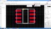
Now its done.....but i had to individually fix the x coordinate of all 4 pads in the right hand column. And had to calculate the position of the first pad that i placed...that is going to be slow..its slower than eagle.

Just copying a column of pads and moving that column 5 mm to the right was not possible,

Using the cross hairs method was not possible to centralize the pads.
 

Attachments

  • soic8.jpg
    soic8.jpg
    576.3 KB · Views: 221
What part of my explanation on how to do exactly this was unclear? Oh, yeah, I did it with a vertical package. Where I said "change the Y coordinates as a group", substitute X. I explained this all, complete with pictures, step by excruciating step.

Regarding centralizing the pads: yesterday, you. complained that you couldn't save a footprint without the software automatically doing this, so obviously this will happen when you save this one also, no?
 
I dont think the "copy a group of pads and move that group x mm in the +ve x direction" has been depicted.

I am trying to copy the attached group of pads and move the copied pads 19mm in the positive x direction...but there appears no way of doing this.
 

Attachments

  • copy pads and move 19mm to the right.jpg
    copy pads and move 19mm to the right.jpg
    406.1 KB · Views: 231
Of course, the real question here is Why are you laying out a standard SOIC-8 package anyway? They are in the EasyEDA system.

The real question is WHY ARE YOU SCREWING AROUND WITH THIS IN THE FIRST PLACE??? The Microchip HV9910B symbol and footprint are already in the EasyEDA library! Search on the part number and it's there. Two seconds of effort to have exactly what you need. So much for conspiracy theories about being forced to use only mysterious LCSC parts.

Time to stop whining, put on your big boy pants and learn how to use the software.

EasyEDA What-the-hell.jpg
 
You can move a group of pads to an absolute coordinate. "No way of doing this" is quickly solved using a calculator.

Perhaps it's time for your employer to find somebody with more flexibility.
 
Last edited:
That's an unusual footprint, but it's simple to make. Each and every pad has its (x, y) coordinates clearly defined. Lay down enough pads for a vertical column, specifying the given drill and annular ring size. Adjust the vertical location of each.

Then copy and paste, and adjust the X location.

Finally, renumber the pads and it's done. In far less than then you've taken writing all these posts that it's impossible.

SmartSelect_20200912-083318_Edge.jpg
 
OK, i see, but i still dont see how to copy a column off pads, and place the copys x mm to the right, and in line such that y coords of each pad are the same as in the original pad column.....

I am not the only one struggling with this......see this video...

...watching from 10:19 to 11:52 and see how he is unable to copy/paste a column of pads, and ends up bodging it.

He finishes off the video by saying."..i hope you find this easier than me!."....he is obviously well struggling with easyeda.

Im searching for a video that shows how to do this properly.

I am fast concluding that there are no good videos on easyeda which show proper custom footprint creation.
 
I have explained it several times.

1. Create one vertical column of pads with the correct positions, drill size and angular ring.

2. Set the SNAP GRID to 1mm.

3. Select the entire column. Press CTRL C. This will prompt for the reference position. Click on the center of the top pad.

4. Press CTRL V to paste the column of pads. Read the cursor position in the box at the lower right of the screen. Click when the Y position is 15, at any convenient X position. (this is why the SNAP GRID is set to 1mm spacing. Set it to 15 if you like.)

5. Change the X coordinate for the entire column (i.e., all pads selected) to the desired value. Repeat this two more times.

6. Renumber the pads in the screwy system used by this part.


I know this works. Because I did it. Less than 30 minutes total.

I am fast concluding that there are no good videos on easyeda which show proper custom footprint creation.

I too am quickly reaching some conclusions. Not about EasyEDA.

EasyEDA Vicor.jpg
 
1. Create one vertical column of pads with the correct positions, drill size and angular ring.

2. Set the SNAP GRID to 1mm.

3. Select the entire column. Press CTRL C. This will prompt for the reference position. Click on the center of the top pad.

4. Press CTRL V to paste the column of pads. Read the cursor position in the box at the lower right of the screen. Click when the Y position is 15, at any convenient X position. (this is why the SNAP GRID is set to 1mm spacing. Set it to 15 if you like.)

5. Change the X coordinate for the entire column (i.e., all pads selected) to the desired value. Repeat this two more times.
Thankyou this was excellent and easy to follow....that job now done.

I am virtually certain to be sacked due to the amount of time, that this is taking me, but just out of interest, where in official easyEDA documentation is your excellent procedure detailed.....i cant find it anywhere?...

Ive just also looked in the manual for where it tells how to import eagle footprints...but it doesnt tell anything.Does the footprint have to be in a PCB layout file first?
 
Last edited:
Just hope your boss doesn't read this thread.

Mike.

He's put in more effort trying to prove EasyEDA can't possibly work than it would have taken to manually place the 56 pads of that footprint. That would be tedious, but not that time consuming.

There are slight differences between Eagle and EasyEDA, but most things are fundamentally the same. I haven't used the current version of Eagle, so I can't comment on the differences, but I find a lot of things easier to do with EasyEDA while I do miss a few features.
 
I find easyEDA lives up to its name. Easy. I found learning Eagle very frustrating, it's not at all intuitive. Maybe now autodesk own it then it'll get better. For now I'm gonna stick with easyEDA.

Mike.
 
Thanks, if the gaffer sacks me tomorrow, then when he asks, why were you slow with easyeda?...ill say..."because the "move column of pads from one position, to another exact position, whilst maintaing their positions relative to each other"...was not explained in the manual.

Though maybe Visitor has saved my bacon, you never know. Thanks.
 
Thanks, if the gaffer sacks me tomorrow, then when he asks, why were you slow with easyeda?...ill say..."because the "move column of pads from one position, to another exact position, whilst maintaing their positions relative to each other"...was not explained in the manual.

Perhaps it would be better to just say it's taken you a while to learn a new software package? Because even with 56 pads to position, doing them one at a time, you still would have wasted less time.
 
Thanks,
Please may i be assisted, i have put a capacitor footprint in the library, and forgot to put details in the "description" field........do you know how i can go back and put stuff in there......?...or do i have to start again from scratch?
 
Status
Not open for further replies.

Latest threads

New Articles From Microcontroller Tips

Back
Top