Continue to Site

Welcome to our site!

Electro Tech is an online community (with over 170,000 members) who enjoy talking about and building electronic circuits, projects and gadgets. To participate you need to register. Registration is free. Click here to register now.

  • Welcome to our site! Electro Tech is an online community (with over 170,000 members) who enjoy talking about and building electronic circuits, projects and gadgets. To participate you need to register. Registration is free. Click here to register now.

Photo+ pcb board etching problem

Status
Not open for further replies.

ozgur84

Member
Hello everybody,

I have a project I have been working on it for a while and now it is the time for producing the pcb board...however, It is not so easy as writing....

I have some positive photoresist coated boards. I did not coat them with positv20 spray or smth similar.

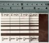
before advancing to the original project, I cut some small pieces of pcb board and tired to find exposure and development times...

I find that, with the black light I have, 12min exposure is necessary. I used a NaOH solution for developing step and after almost 2min the patterns were nicely observable on the board.

as the final step I etch the board with Fe3Cl solution. however, it does not go further even though I waited half an hour and put the container in a hot water bath. there are some areas close to the board edge where were partly etched and some spots on the board. put the pattern is not appearing.

the situation makes me quite curious because the main project is a double sided board...

So, I would like to hear your ideas.
 
The most likely cause for that is under exposure. It could be underdevelopment, but as we know nothing about the particular products you are using, it is hard to say. I doubt it is underdevelopment.

With my photoresist, the exposed areas turn purple when exposed to the NaOH developer. Did yours do the same? Was all the purple gone before you tried etching?

To check for underdevelopment, take one of your scraps that didn't etch, put it in bright sunlight for 15 minutes. Then try your developer on it. If more resist is removed (i.e., you get a purple color), then underexposure is the culprit.

Another way to test for underexposure is to put the scrap in more concentrated NaOH (like you will be using at the end to remove all resist), rinse, and put in FeCl3. If the netal now etches, it was probably underexposure.

You say "blacklight." Please be more specific. What bulb did you use? How is it labeled? How close is the bulb to the PCB? What wattage?

John

ok, I start with the bulb. it is a 75W UV active bulb brand is omnilux. I exposure from 15cm distance.

the exposured resist turns into not purple but orange-dark brownish color and masked sites stays yellowish after developing with NaOH (10g/L) solution.

I also bought sodium persulfate today and it worked with some scraps but the etching rate is still so slow in spite of the hot water bath and the traces are not well resolved...

I also tried 30min exposure and after that the development was rapidly quick, the traces have disappeared before I decide it is enough or not...

Now I try 45 min exposure, I suppose I will get the result in one hour
 
Can you provide a link to the exact light that you are using? I could not find "Active" style on its site.

What brand is your photoresist? What do its directions say to use for developer?

John
 
Can you provide a link to the exact light that you are using? I could not find "Active" style on its site.

What brand is your photoresist? What do its directions say to use for developer?

John

https://www.thomann.de/gb/stairville_xpw400_uv_lampe.htm this is the same brand but the one I have is 75W instead of 400 in the link.

I suppose the boards are "Bungard" but i am not sure because there is no brand on them and the guys at the store also could not inform me about the brand or process.

There is no brand for developer, it is granulated NaOH from a laboratory supplier...

Bad news, because the lamp is so powerful the transparency masks were melted:( now I am trying my reading lamp with a regular 25W bulb (not UV) I will double the exposure time, something like 1.5 hour...I read in the forum that somebody already succeeded with a regular lamp...
 
Do a test board and use a few different exposure times masking off different areas. Also have a small part of the board where you take off the photoresist with a bit of acetone or similar.

It sounds to me like the copper isn't being totally and cleanly exposed to the ferric chloride - even a bit of grease on it will slow down the etching so if the photoresist isn't completely removed it won't etch properly.
 

Attachments

  • testpcb.jpg
    testpcb.jpg
    106.7 KB · Views: 230
As for the lamp, I didn't find what I wanted to know. The rating is 75W, which is probably just its power consumption. We don't know the source of the UV and so don't know what the spectrum of light is. The positive photoresists we use will work with light into the near UV.

Did you cover the plastic sheet with a glass plate to keep it flat?

I am still leaning toward under exposure. In other words, only the top layers of resist are getting enough light to become soluble in the alkali, and a thin layer of unreacted resist remains on the board that is blocking etching.

When you first placed the board in the ferric chloride, did the board turn a salmon red? Did the ferric chloride wet the surface or bead up?

John

I saw that the lamp has a spectrum around 400nm and if the pcb boards are the ones which I thought they are, the max spectral sensitivity of the photoresist is around 400nm. It might work.

I put a glass plate on the surface to keep the mask flat this time.

When I dipped the board into Fe3Cl it did not react rapidly (it was not so hot tough, it was around the room temp.). Now I want to use sodium persulfate instead. I have not good feelings about the Fe3Cl which I use... It was granulated and I prepared the solution, the one I used couple of years before were more powerful and it used to dissolve more copper with higher reaction rates.
 
400 nm light if fine. The resists have a photosensitizer in them that allows longer wavelengths to be used compared to what one might suspect from the resin itself.

I was worried the wavelength was too short, which can cause unwanted reactions to occur. The glass plate pretty much guarantees that is not the case.

If it doesn't etch with ferric chloride or even turn that salmon color, I doubt the persulfate will work either. You say the ferric chloride did not react rapidly and mention a little etching around the edges. The fact that there was any etching around the edges pretty much proves the ferric chloride is OK and the problem you have is in exposing the resist and /or developing it.
John

I agree, there is something wrong with the developing process. an overdeveloped scrap sample was etched fine. It took almost two hours to get there but somehow it worked...
the picture is here
15022013072.jpg

But the problem is, I can not replicate the result somehow and there is no guarantee which it will work when I exposure the two sided copper:mad:. I wish I could have made the laser printer based masking worked.
 
I have an urgent question! I make it worked for one side. I have just exposed one side 30min with desk lamp and 1hour with UV lamp. The other side is exposed only with the UV lamp. I took the board out and put it into the developer solution and first site (exposed with both lamps) reacted fine the excess resist went away rapidly and now I see the pattern but the other side is as it has never been exposed. Can I go on exposing the the back side?
 
What is your artwork on? Paper or transparency?

Those are very long exposure times. I use around 50 seconds with LEDs at 30cm (using Positiv 20)
My developing time is around the same.

Etching depends on whether I remember to keep it warm or not, but varies between 20 minutes and an hour.

If this is your first attempt, don't worry, it will soon become second nature, but it does take practice. Like many things, reading what to do, and the actual doing are only loosely connected.
 
Almost certainly yes. Besides,what have you got to lose?

Go for it!

John

Yea I tried and it was promising, I will try it again with some test samples to find out the exact exposure mechanism with my tools.

This is the picture of better exposed (first site) after developing with NaOH. What do you think?
16022013080.jpg

The other side which exposed multiple times is not so promising. I can not demonstrate so much with a picture because the pattern is not visible like the previous one.
 
Today I also tried the contact printing for the same artwork. I got the design printed in a copy center and ironed to a normal copper double sided board. I prepared a Sodium persulfate solution with 300ml water and almost 80g sodium persulfate (I also added more during the process) at aprox. 60 degree Celcius. I etch the board in 15 min. here is the result.
**broken link removed**

Because the ink polymer broadened during the ironing the result is not satisfying but it will work :) I made some scratching afterwards.
 
What is your artwork on? Paper or transparency?

Those are very long exposure times. I use around 50 seconds with LEDs at 30cm (using Positiv 20)
My developing time is around the same.

Etching depends on whether I remember to keep it warm or not, but varies between 20 minutes and an hour.

If this is your first attempt, don't worry, it will soon become second nature, but it does take practice. Like many things, reading what to do, and the actual doing are only loosely connected.

Hello Sangoma, I would like to hear about your exposure set-up. I might build one for myself, obviously my current lamp is not working properly for this specific purpose... I am also planning to use positiv 20 spray instead of an (quasi)unknown photosensitive board...

By the way, the artwork is on transparency.
 
Last edited:
@Post #14

I use Injectorall sensitized boards. If that photo was one of mine, I would say it is under exposed or under developed. Although the photosensitive layer is quite thin, with reflected light, one can see ridges around the protected areas, which are not evident in your photo. Put a drop of ferric chloride on a clear area, wash it off, and check for any color change or sign of etching. Even simpler, let water run over the board and see if it is wetted. If the water beads up over the clear areas, then you still have resist present.

@Post #15

Invalid link.

@Post #16

Have you considered just getting the usual fluorescent bulbs? The type I use are labeled "BL." With just one 15W bulb about 4" (10cm) away, my exposure was 12 to 15 minutes. I used a reflector made of aluminum foil that just lay on the bulb. Almost any white fluorescent bulb will work. They also put out a lot less heat.

Is the glass you are using ordinary single-pane glass or is it coated in any way, say to be non-reflective?

John
 
Last edited:
I use 60 UV LEDs, no box, just hold them about 30cm above the board and move them around a bit to get even exposure. It works fine for boards up to 10X16 cm, I plane to make another set if I want to do larger boards.

You need to check the specs of the LEDs and make sure the wavelength matches the resist. Got them on fleabay, quite cheap.
I'm doing a similar thing with an old scanner (when I get some time !) - doing a staggered row of UV LEDs and moving them with the scanner mechanism over the exposed area.
 
@Post #14

I use Injectorall sensitized boards. If that photo was one of mine, I would say it is under exposed or under developed. Although the photosensitive layer is quite thin, with reflected light, one can see ridges around the protected areas, which are not evident in your photo. Put a drop of ferric chloride on a clear area, wash it off, and check for any color change or sign of etching. Even simpler, let water run over the board and see if it is wetted. If the water beads up over the clear areas, then you still have resist present.

@Post #15

Invalid link.

@Post #16

Have you considered just getting the usual fluorescent bulbs? The type I use are labeled "BL." With just one 15W bulb about 4" (10cm) away, my exposure was 12 to 15 minutes. I used a reflector made of aluminum foil that just lay on the bulb. Almost any white fluorescent bulb will work. They also put out a lot less heat.

Is the glass you are using ordinary single-pane glass or is it coated in any way, say to be non-reflective?

John

I think I will not used that pre-coated boards, the one in the picture was exposed more than one hour both with the desk lamp and the UV and I still do not have the exposure that I want... tomorrow I will try this Fe3Cl test and I will write the results here.

About contact printing...I might have over-ironed the transparency. because the conductive lines were broadened after ironing. However I carved the connected parts due to broadening and soldered the components, the board seems fine. tomorrow I will connect the switches and motor and I will try the performance

Is your fluorescent bulb one of these energy-saving lamps or a bar type? I know that the energy-saving bulbs emit significant amount of UV. it can be an option and worth to try.

There is no special coating on the glass plates.
 
Status
Not open for further replies.

Latest threads

New Articles From Microcontroller Tips

Back
Top