Electro Tech is an online community (with over 170,000 members) who enjoy talking about and building electronic circuits, projects and gadgets. To participate you need to register. Registration is free. Click here to register now.
Welcome to our site! Electro Tech is an online community (with over 170,000 members) who enjoy talking about and building electronic circuits, projects and gadgets. To participate you need to register. Registration is free. Click here to register now.
Just wondering what everyone recommends as a good pad n track size to use for boards created using usual laser printer transfer onto copper then etch at home?
No special components, just standard DIP's, Resistors, Axial Caps, etc...
popular ones to use is Eagle and expresspcb.
some even use sprint
size of traces depends on your experience in DIY boards and how much current the traces and type of signal they are to carry
Most of the boards I etch I use .25 inch wide traces and the pads are what is the default for each componet.
I use expresspcb.
Im using Protel 99, the circuit im building is a simple 5W amp. The pads for the DIP that im using are 65mil x 100mil oblongs. The tracks i have set to 15mil. Is that enough? Is there a chart or anything that will tell you the recommended size of trace for the current it has to flow?
There are at least 2 web sites with calculators for determining trace width for current. Google for "trace width".
In general larger traces are easier then smaller ones. Start wide and big and move down as you become more confident. 15 mil is OK but I would go to 24 mil for power traces. Both are possibly overkill but if you have the room why not.
In the past we have helped a number of people with their first layout. Feel free to give it a try and attache it to a post in this thread. We will be happy to give you some pointers.
While making hair thin tracks and tiny pads looks "high tech" it can cause you a lot of grief in a home built board, when tracks burn up (from faults) and pads lift off the board when unsoldering parts.
Make everything as big and wide as possible, especially on an experimental prototype.
Sometimes thin tracks are the only way for very dense layouts. But if you can make it big, and have the space to do it, then it makes a much more robust board.
I made that mistake once and used .25mm traces and not .025 inch.
BUT in my defense I purposelessly made some .006 traces and they came out really fine and had continuity the entire length. I made some boxes around my design using .006. The Pulsar website mentioned being able to run two traces between IC pads.
BUT found out that using 2 oz. boards is a mistake unless your making really wide traces.
Two traces between IC pins would sometimes solve routing problems.
0.006 inch trace width is about that of main boards. Using that trace width requires a grid size of 1 to 2 mils (and a monitor of at least 22 ") to pass the DRC without error message. Maximum available space between traces and pads is 0.21166mm.
If you need to route traces between pads you can go with .016 inch traces and reduce the with of the segment that goes between the pins to .01 inch or smaller.
Pulsar states that it can be done!! what about 1/2 ma is all it could carry--lol
I'll stick with .025 and if need be .015.
I set my printer for 1200 dpi and didn't see any difference between 1200 and 600? or is it 800??
need to look at this again.
Use a transparency to print. Put it on a light table and look at the traces using a microscope. You'll see the blank areas within the trace pretty well.
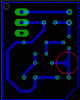
This is what i whipped up in Protel 99. All tracks are 25mil and a gaps are set to 15mil. I used polygon fill around the DIP and the power part of circuit to help with heatsinking as suggested by Audioguru. Look ok?
the layout looks ok but get rid of all the T traces.
I usually just fill the corners with a filled 45 degree angle
what is it, trace wideth etc details.
also note that some laser printers (assuming your doing direct etch) won't keep up when applying lots of ink in large areas.
a cross hatch area fill will usually work as good.
This site uses cookies to help personalise content, tailor your experience and to keep you logged in if you register.
By continuing to use this site, you are consenting to our use of cookies.

")