Continue to Site

Welcome to our site!

Electro Tech is an online community (with over 170,000 members) who enjoy talking about and building electronic circuits, projects and gadgets. To participate you need to register. Registration is free. Click here to register now.

  • Welcome to our site! Electro Tech is an online community (with over 170,000 members) who enjoy talking about and building electronic circuits, projects and gadgets. To participate you need to register. Registration is free. Click here to register now.

New here and I need help

Status
Not open for further replies.

Tunaman

New Member
Hello all. Thanks in advance.
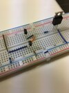
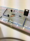
I have this battery charger. It is for charging a NIMH 16.8v 720mAh battery. Every one of these chargers fails in the same way. Seems like a direct short and the Mosfet blows and gets very hot. I have removed every component on the board just to familiarize myself with soldering these little parts. I tested every component I know how to, except for the MC34060AD and the BQ2002sn chips. I dont know how to test those. I am sure for you guys this is a cakewalk. These little chargers cost me 80 bucks to buy. I have a bunch of dead ones and all the parts to fix them. If someone could teach me how to troubleshoot this little board I would be forever indebted. On a good one, we put 12v 1500ma power input and the output to the battery is usually 20+volts. Here are some pics of this board. I have removed the Mosfet and LED in one of the pics.
IMG_1110.JPG
IMG_1109.JPG
IMG_1111.JPG
IMG_1112.JPG
 
Last edited:
Can you post a photo of the board underside as well?

In a failed one, can you test the two transistors at the bottom left, next to the power input socket? Those look to the the gate drivers for the MOSFET.

A power FET with higher current and voltage rating may work, but would also need higher current gate drive, as the FET gate capacitance is also higher.
 
I have included a picture of the bottom of the board. If I understand you correctly there is a way to "beef up" this mosfet and diodes? Excuse my ignorance but I dont think I am good enough to figure out which parts to use for this upgrade. Can you suggest replacements? My sincere thanks to you for helping me out. I have already ordered the 3906 and 914 to replace these. Both transistors appear to be non working. I only have the Bside transistor tester to go by. I will have a more definitive answer after I have a new one to compare it to.
 
That's the idea, use somewhat more rugged parts and see if they survive.

I'd guess the 3906 is a 2N3906, but what have you ordered for the "914" ??
[Edit - just looked at the PCB pattern again and realised its a diode, so 1N914.]

Can you please add another photo of the PCB topside, with better lighting around the area near the power input connector? I'm trying to trace connections and that area is in shadow. I think I have it right, but just want to be certain.
 
Last edited:
Do you have access to a working device?
If so,then test a known good unit compared to a non working one to narrow the search for the bad component.
 
Thank you so much for the replies. Here is a better picture of the topside with all components removed. I believe the 3906 is a MMBT3906 as it has a marking of 2A. SOT-23 is the package size.
There are 2 914 packages and I believe they are the MMBD 914 type with a marking of 5D. Also SOT-23 package size. As soon as these parts get here I will have a known good to check against. As I mentioned before, these chargers have been blowing up for years and the only option right now is to buy a new one. If I could beef the up it would be a godsend. Also...on the lower right side of the board, to the left of the BQ2002sn chip there are 2 Caps...size 0603. The bottom most cap is marked 10nf and reads that when I check it. The cap directly above it is the only cap on the board that is not 10nf with the one single exception of a 1nf cap. I cannot make out the marking on the board to determine what size it is but it reads 103nf when i check it. I dont know if that is right or wrong. Thanks for all of your input.
IMG_1118.JPG
 
Last edited:
Do you have access to a working device?
If so,then test a known good unit compared to a non working one to narrow the search for the bad component.
Actually I have found the bad component...the IRF 520 Mosfet. The reason for this thread is that I am trying to find out WHY they are blowing and what if any parts I can upgrade to stop this from happening. Thank you for your input.
 
A possible reason for the IRF520 to blow would be a low gate voltage (less than 10V), causing the RDSon to be higher, creating more heat and thus destroying the MOSFET which has no heatsink.
Other possibility is a short circuit on the output, again causing maximum current and heat that cannot be dissipated without a heatsink.
Reverse polarity may cause damage, depending if the input protection diode works (914 device?). Hard to tell.
Without a schematic, hard to really diagnose the problem. Test each component, then check the input voltage/polarity and then test the output voltages. Check the gate voltage.
This seems to be a switching regulator of some sort, the IC may be the problem if it is not regulating properly or has gone "bad". Also, back EMF from the inductor could cause a problem if the back emf diode (5819?) is bad.
Good luck...
 
Excuse my ignorance but I dont think I am good enough to figure out which parts to use for this upgrade. Can you suggest replacements?
OK, this is what I'd suggest:

The left side is the FET drive circuit as it is; it uses the output transistor in the IC as the positive gate drive via the diode & when that switches off, the 1K pulls the bas of the 2N3906 to ground, giving a fast discharge.

Higher rated FETs have higher gate capacitance, so would switch rather more slowly with that circuit, making them lossy. The right hand version uses two transistors to allow high current both for charging the gate as it switches on and discharging it at switch off; the 22 Ohm resistor limits the peak current to safe levels.

That should allow for a much higher rated FET.

The output diode also needs upgrading, it's only a 1A one which is dodgy in itself to me.

I've show it with ZTX851 & 951; it does not have to be those, but definitely some transistors with decent gain and 1A or more current rating.

BoostChargerMods.jpg
 
Thank you so much for the reply. I just have a couple of questions. You stated that I should replace 2 transistors with a ZTX851 and 951 but I dont see the 951 on your schematic. Shall I remove the 914 diode completely and just use jumpers to create the new transistor path? Shall I keep the 3906 intact or change that one to the 951 you dont show? Thanks for putting up with my lack of knowledge.
 
You stated that I should replace 2 transistors with a ZTX851 and 951 but I dont see the 951 on your schematic.
Sorry, my mistake - I meant to rename the 2N3906 to ZTX951 in the right hand diagram...

Remove the diode; the two transistors have both the their bases and emitters commoned, so just four connections total.

Three of those can connect to the existing transistor / diode pads and the upper collector needs a link to positive at the power socket.
 
Again I thank you for the reply. I have but one question left about the 22ohm resistor. Any specific type? and it goes inline between the gate of the IRF640 and the common emitters of the 2 new transistors? All of the existing resistors stay? Thanks so much.
 
OK, a quick back-of-a-beermat grade connection scribble for the transistors, viewed from above (ie. leads underneath them):

BoostChargeraddon.jpg


The ZTX851 is the NPN one at the top, and ZTX951 PNP at the bottom.

And the PCB connection points:
Red: V+
Blue: 0V
Green: PWM from IC (In to transistor bases)
Yellow: FET gate (Out from 22R resistor).

The original 1K resistor needs to be left in place between green and red.

And don't forget to use a higher rated power diode in place of the 5819; any point of failure could cascade through and blow the FET again.

Charger_PCB_connections.jpg
 
OK. Thanks so much again. Now the only problem I have is that the ztx851 and 951 are TO 92 package type and the ones I am replacing are SOT 23. This board sits in a plastic case that leaves 1/2" if space before the cover goes on. Any help on a way find SOT 23 comparable transistors or if anyone can offer up a solution in soldering these together so I dont short this whole mess out. Is it generally ok to shorten the leads on the TO92 package so i can get them in there? Thanks in advance. You guys have been terriffic so far. I almost have this licked.
 
Is it generally ok to shorten the leads on the TO92 package so i can get them in there?
Absolutely - shorten them, bend them to suit & also try and put a short sideways bit at the end of each that will attach to the pcb, to give more area where the lead solders to a pad.
 
Well I think I have done it correctly. I'll be soldering this up as soon as the transistors get here.. Let me know if you think I got it right. You guys are the best. Thanks so much.
 

Attachments

  • IMG_1122.JPG
    IMG_1122.JPG
    1.3 MB · Views: 197
  • IMG_1123.JPG
    IMG_1123.JPG
    1.2 MB · Views: 195
I think you are missing the link from the blue input wire to the upper base? Looks OK other than that.
 
"The original 1K resistor needs to be left in place between green and red."
I am sorry, but did you mean between green and blue? I believe it goes from green to blue jumping over the yellow trace. That is where it was originally. Thanks
 
Status
Not open for further replies.

Latest threads

New Articles From Microcontroller Tips

Back
Top