Continue to Site

Welcome to our site!

Electro Tech is an online community (with over 170,000 members) who enjoy talking about and building electronic circuits, projects and gadgets. To participate you need to register. Registration is free. Click here to register now.

  • Welcome to our site! Electro Tech is an online community (with over 170,000 members) who enjoy talking about and building electronic circuits, projects and gadgets. To participate you need to register. Registration is free. Click here to register now.

NAND Gate

Status
Not open for further replies.

sxy

Member
Hi
Can anyone explain to me the attached circuit how NAND gate works in this particular circuit?
thanks a lot
 

Attachments

  • NAND GATE1.jpg
    NAND GATE1.jpg
    320.3 KB · Views: 211
Isn't it obvious?
The positive power supply voltage is not shown.
 
Yet another really bad circuit, as voltage-wise, it is a simple diode logic AND gate.

The LED with its series resistor is connected between output and power rather than output and ground, so it lights when the output is low.

This is a true diode (actually DTL, diode-transistor logic) NAND, with the transistor inverting the output of the diode AND section:
 
You don't say where the design comes from, but wherever it is, they are incorrect. In positive-true logic, that is an AND circuit, not NAND.

If you consider both the inputs and outputs to be negative-true, then it is an inverting-input NOR gate: if either input goes low, the output goes low.

ak
 
Since you did not provide a link to this other video, we'll have to take your word for it. Apparently, in addition to the 1,800 views of the first video, there are another 100,000 people with bad information. Or there are 99,999 people who know better.

ak

1652584894303.png
 
The problem is the LED column. His listing of when the LED is on or off is correct, but the indicated logic level (1) is incorrect. As is clearly indicated by the schematic, when either input is low, the output is at a low voltage level, a logic 0. This turns on the LED because the anode of the LED is connected to a high voltage level (9 V) through a 1 K resistor. When a low level is the state that does something, this is called negative logic.


Such an output signal is called an active-low output.


When you correct the logic level for what the circuit actually does, the table is that of an AND gate. This was worked out before the US civil war, back in the 1850's.


ak
 
Last edited:
Thanks a lot!
So watch the other video with detailed explaination:
Here is the link to the video:
thanks
 
The same configuration of NAND exists in video of 100;000 views.
thanks a lot
And there are many other wrong-due-to-ignorance, deliberate misinformation or just made up comedy videos with millions of views each.

Something being on youtube - or even in a textbook - is not proof of accuracy or correctness. There are vast quantities of example circuits & devices on the internet that are not what the posters claim.


The visual effect may be NAND, but only because the LED is connected to light when the output is LOW.

The gate logic itself is AND. Put a voltmeter on the various points and see for yourself!

The inverse logic function of an AND gate is OR. That's how that circuit functions - connect input 1 OR input 2 to 0V and the LED lights as the output goes low.
 
He explains in the video what happens when the inputs of NAND is:
a=0 b=1
or in case of:
a=b=1.
thanks a lot.
 
And the second video is another confusing / misinformation one.

The poster is using active high logic for the inputs and active low output. That is not a valid logic setup.

For any "gate" to be valid and functional, it must be possible to connect on to more gates built in a similar way. None of the ones you have posted would work like that.

That is functionally an inverse logic AND. Both inputs must be low for the output to be low and the LED be on.

The posters may well be demonstrating logic concepts, as far as the input switches an LEDs are concerned.

BUT - the gate "circuits" are not actually what they say they are, as the LEDs are connected to turn on with low [0] logic output rather than high [1] logic output.
 
These are real-world diode logic gates - a schematic of one of the logic boards from the first mass-production computer, back in the early 1960s.


That particular board has three gates which can be used as NAND (active high logic) or NOR (active low logic), plus some spare loads & biasing.

The entire computer was built with this style of logic system, no integrated circuits at all. Note that the transistors are PNP so polarities are reversed compared to what you would expect with modern devices using NPN transistors.

(If you are wondering how a complete computer was built with such simple logic boards - it had lots of them. in many types, in a large double-sided cardframe!
https://jeelabs.org/article/1607a/ )
 
I had the district displeasure of interfacing with a PDP8 using paper tape to input programs,
for IC test purposes. Then with a PDP11 (I think) with a disk pack. Had one blow up with my head
inches away from stack. But to the DEC EEs credit (someone must have gotten injured), it had a
rugged housing to contain the shrapnel.

Good times.

DIY PDP8 - https://hackaday.com/2015/03/26/hackaday-retro-edition-remaking-the-pdp-8i-with-a-raspberry-pi/
Cool - scary to think though that something as small and cheap as a PI can simulate (and greatly exceed) a PDP8.
 
Several decades ago, when I was still living at my parents place, I managed to acquire a PDP8 that some part of Nottingham, university was scrapping.
That, together with the ASR33 and a lot of other vintage radio & computer gear unfortunately had to go when I moved out to a bedsit.

So ever since, I've been interested in the various rebuild / replica projects - and that one was too good to miss!

PiDP8.jpg
 
Here is the link to the video:
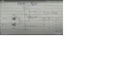
At 16:48, when the NAND drawing is complete, notice that in the LED column there are *no* logic levels. He has On and OFF, but no 0's and 1's. This is the only reason his statements are correct. Also, it is a significant omission, and throughout the video he bounces back and forth between active-high and active-low outputs without a word of explanation. In a world where everyone assumes that, unless stated differently, all logic is positive logic and all inputs and outputs are active-high, this is a critical error.

Note that the standard logic symbols for NAND and NOR gates have bubbles on the outputs, and the DeMorgan equivalents have bubbles on the inputs. These are the indicators that negative logic and active-low signals are at work.

For both the NAND and NOR functions, his truth tables are not correct. To see this, remember that the only difference between a NAND gate and an AND gate is an inverted output. A NAND gate is literally two gates in series, an AND gate and a NOT gate, also called an inverter. If you replace the words On and Off with the logic levels 1 and 0 in the AND and NAND tables, you will see that the NAND output column is not the simple inversion of the AND output column.

One last thing: The reason he gets away with his sloppy presentation is that he is inconsistent with the LED connection:

A) Sometimes the LED anode is connected to Vcc with the inputs driving the cathode.

and

B) Sometimes the LED cathode is connected to GND with the inputs driving the anode.

This is what makes this video very, very wrong - he flips back and forth between two logic conventions without any explanation, implying that the two are equivalent. They.Are,Not. Option B is the correct way to indicate positive logic and active-high conditions. If he sticks with this for all four gate types, two of them will not work. That is, the truth tables with 1's and 0's in the output column will be correct, bot the LED indications will not.

ak
 
Last edited:
Status
Not open for further replies.

Latest threads

New Articles From Microcontroller Tips

Back
Top