Jugurtha
Member
So I had a flu… Wouldn’t go out.. Couldn’t anyway… And decided to learn CadSoft Eagle.
I opened a thread about Microcontrollers recently, and I wanted to build a PIC Programmer … I’ll eventually buy one (PICKit 2 or something), I just wanted to lose my PCB virginity with this project.
Anyway, I wanted something simple, so I exluded de facto clones with microcontrollers which have to be programmed in the first place inside them
(The ones I found had a PIC18 inside, like PICKit2 clones).
Anyway… Eagle thingy..
The project I chose is a JDM Serial PIC Programmer… (JDM stands for Jens Dyekjaer Madsen) which I found here :
http://webspace.webring.com/people/jl/leon_heller/pic.html
And which the author found here :
**broken link removed**
He substituted the 25 pin connector with a 9 pin connector ( DB25 – DB9 … RS-232) .. I like the DB9 more.
I worked with the schematic from the original page. Have in mind though that pins like TxD (2) or GND (7) refer to the DB25 Pinout, while I’m going to do a DB9 version.
To get the corresponding pins in a DB9, you can search for something like « RS232 pinout » or « DB9 pinout » or something like that..
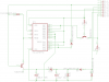
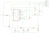
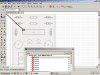
Anyway … Here are schematics I did…
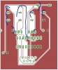
Serial JDM PIC Programmer_Rev1.1.png
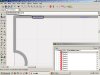
Serial JDM PIC Programmer_Rev1.4.png (Notice how angles are « rounded », it’s called « Mitering », there’s a button for it on the left)
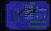
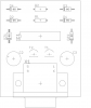
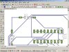
Here’s ultimately the « Board », revision 4… The file named "General.png". Not all layers are displayed here.
I drew a rectangle on the whole surface on vRestrict, I didn’t want any Vias in there. I’m a beginner, so I didn’t want to do that yet.
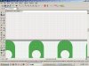
I drew two small rectangles under the PIC on two layers tRestrict and bRestrict, they’re a match. I didn’t want any routing under the PIC, because I thought it would better (Less heat influencing its functionning, and I wanted to diminish the influence of a field that would be created by the the current in a hypothetical route.)
I had a problem as shown in the image, where these rectangles crossed over the pads, and it showed errors when I hit DRC (Design Rules Check).
I couldn’t draw accurate enough rectangles to include the whole chip, so I increased the Grid resolution by chosing 5 mils in « Size ». I could draw more my rectangles with more precision.
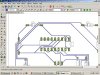
I think I managed to have a single sided board before (drawing a rectangle in tRestrict that included the whole surface), but NOT with that disposition. This one is very symmetrical as you can see here :
Not very big board, 1.8’’ by 2.135’’.
My questions are :
1. Concerning the schematic : Are there guidelines or Good practice rules or something ? I know I can make Non visually connected components to make things « neat », but as long as it’s not complicated, I prefer to « see » the flow of current and stuff… But anyhow, is there something that can be improved in the schematic ?
2. Am I thinking too much about the board ? Protecting the chip from stuff and all ?
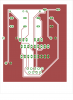
3. I can do « Copper Pouring » for say Ground or in my case N $3 ‘because it’s used a lot ‘. I think that i twill spare some un-necessary etching and will save etchant (Less copper to etch, less molecules of etchant will be used, so quantity of etchant will last longer, etc)… How would these « planes » affect the functionning of the board practically…Any unliked capacitive effect or something ? How bad is it ?
I know it’s been only a day since I’m using Eagle and I’ll discover stuff as I work with it and make boards. I’ll start making them as soon as I can.
Thanks,
~Jugurtha Hadjar,
I opened a thread about Microcontrollers recently, and I wanted to build a PIC Programmer … I’ll eventually buy one (PICKit 2 or something), I just wanted to lose my PCB virginity with this project.
Anyway, I wanted something simple, so I exluded de facto clones with microcontrollers which have to be programmed in the first place inside them
(The ones I found had a PIC18 inside, like PICKit2 clones).
Anyway… Eagle thingy..
The project I chose is a JDM Serial PIC Programmer… (JDM stands for Jens Dyekjaer Madsen) which I found here :
http://webspace.webring.com/people/jl/leon_heller/pic.html
And which the author found here :
**broken link removed**
He substituted the 25 pin connector with a 9 pin connector ( DB25 – DB9 … RS-232) .. I like the DB9 more.
I worked with the schematic from the original page. Have in mind though that pins like TxD (2) or GND (7) refer to the DB25 Pinout, while I’m going to do a DB9 version.
To get the corresponding pins in a DB9, you can search for something like « RS232 pinout » or « DB9 pinout » or something like that..
Anyway … Here are schematics I did…
Serial JDM PIC Programmer_Rev1.1.png
Serial JDM PIC Programmer_Rev1.4.png (Notice how angles are « rounded », it’s called « Mitering », there’s a button for it on the left)
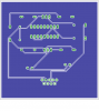
Here’s ultimately the « Board », revision 4… The file named "General.png". Not all layers are displayed here.
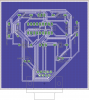
I drew a rectangle on the whole surface on vRestrict, I didn’t want any Vias in there. I’m a beginner, so I didn’t want to do that yet.
I drew two small rectangles under the PIC on two layers tRestrict and bRestrict, they’re a match. I didn’t want any routing under the PIC, because I thought it would better (Less heat influencing its functionning, and I wanted to diminish the influence of a field that would be created by the the current in a hypothetical route.)
I had a problem as shown in the image, where these rectangles crossed over the pads, and it showed errors when I hit DRC (Design Rules Check).
I couldn’t draw accurate enough rectangles to include the whole chip, so I increased the Grid resolution by chosing 5 mils in « Size ». I could draw more my rectangles with more precision.
I think I managed to have a single sided board before (drawing a rectangle in tRestrict that included the whole surface), but NOT with that disposition. This one is very symmetrical as you can see here :
Not very big board, 1.8’’ by 2.135’’.
My questions are :
1. Concerning the schematic : Are there guidelines or Good practice rules or something ? I know I can make Non visually connected components to make things « neat », but as long as it’s not complicated, I prefer to « see » the flow of current and stuff… But anyhow, is there something that can be improved in the schematic ?
2. Am I thinking too much about the board ? Protecting the chip from stuff and all ?
3. I can do « Copper Pouring » for say Ground or in my case N $3 ‘because it’s used a lot ‘. I think that i twill spare some un-necessary etching and will save etchant (Less copper to etch, less molecules of etchant will be used, so quantity of etchant will last longer, etc)… How would these « planes » affect the functionning of the board practically…Any unliked capacitive effect or something ? How bad is it ?
I know it’s been only a day since I’m using Eagle and I’ll discover stuff as I work with it and make boards. I’ll start making them as soon as I can.
Thanks,
~Jugurtha Hadjar,
Attachments
-
 Serial JDM PIC Programmer_Rev1.1.png42.9 KB · Views: 512
 -
 Serial JDM PIC Programmer_Rev1.4.png43.3 KB · Views: 572
 -
 General.png7.8 KB · Views: 359
 -
 tRestrict, bRestrict Under PIC.JPG170.6 KB · Views: 377
 -
 N$3_Copper_Pouring_Top_Layer.png73.1 KB · Views: 378
 -
 Restrict_Error_Layer_16.JPG123.4 KB · Views: 401
 -
 Restrict_Error_Layer_16_Zoom_In.JPG156.3 KB · Views: 423
 -
 Ripup_and_Route_Again_Previous.JPG86.9 KB · Views: 344
 -
 Ripup_and_Route_Again_Next.JPG87.7 KB · Views: 341
Last edited: