Continue to Site

Welcome to our site!

Electro Tech is an online community (with over 170,000 members) who enjoy talking about and building electronic circuits, projects and gadgets. To participate you need to register. Registration is free. Click here to register now.

  • Welcome to our site! Electro Tech is an online community (with over 170,000 members) who enjoy talking about and building electronic circuits, projects and gadgets. To participate you need to register. Registration is free. Click here to register now.

Multiple pour areas on one layer DS

Status
Not open for further replies.

ThomsCircuit

Well-Known Member
I just want to be sure im not using the pour feature in a manner it was not intended for.
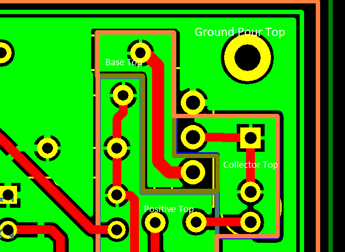
This transistor here can benefit from wide tracks so i created small pours to accomplish this.
There are 4 separate pours on the (TOP) side and a full GND pour on the bottom layer.
Ive labeled them in this image.
Want to be sure that i have utilized the feature correctly to accomplish my goal which is to create the widest plane possible for the track in question To also create as many spokes as possible so soldering is successful.
pmw fade PCB Copper2.png
 
Well you're sort doing it upside down, the ground plane usually goes on the top, with (most of) the tracks on the bottom. I usually put the ground tracks on the top as well, then when you do the pour it incorporates the ground tracks in the ground plane. I've never seen any reason for multiple pours, and I'm not even sure Designspark allows it? - or any reason to want to?.

One of the points of the ground plane is to screen the components from the tracks, so placing the ground plane on the bottom of the board makes it somewhat pointless.
i read an explanation about the interconnect tracks being on the bottom on another post. That the insufficient flow of solder in the holes from the bottom to the top of the board could cause problems and I have seen this in my work so i can agree that the reasoning has merit but this is how i was shown how to create PCB.

Now for the question at hand. DS ver 10.0 did allow me to place these pours on the board. I applied the pour and it did what it is supposed to do. So for the reason that I am using the pour feature is to make the tracks wider without breaking the "Drill back out hole rule" you say is not necessary. Is there another way to make the tracks wider without breaking any design check rules?
 
i read an explanation about the interconnect tracks being on the bottom on another post. That the insufficient flow of solder in the holes from the bottom to the top of the board could cause problems and I have seen this in my work so i can agree that the reasoning has merit but this is how i was shown how to create PCB.

I've never heard of or seen any such thing, I suggest you try looking at professionally made PCB's used in electronic items you might have, none of which look anything like yours.

As for the 'drill back out hole rule' simply disable it (untick it), the PCB's are perfect when that's done - and I'm fairly confused as to what it even means?.
 
the ground plane usually goes on the top
There are a million different way.
I have done Ground on one side and power on the other with traces in the middle. (4 layer board) In that case I am trying to shield the traces in a copper box.
I have put the Ground and Power in the middle and run the traces on the outside so I can trouble shoot. (cut and patch traces)
With through hole parts I normally put the traces on the bottom side.
With surface mount parts I keep the traces on the top with the parts so I don't have vias. (ground on bottom)

Do what you want. Just have a reason for doing it.
 
Im not posting this because i disagree. Im posting this because its part of the PCB program. They provide an explanation for what happens when tracks are too wide. Now i understand that there are standards. Just as there are standards for soldering components. and even the sloppiest of solder jobs can somehow work. This could be just one of those things that doesn't really cause problems but we're obligated to document them.

Now my point is this.
Making a track (trace) that is compatible with the hole then adding a pour to the trace to make it wider than the hole but still follow the design rules appears to me as a solution to my problem. However are copper pours used for this purpose? I did find an article that list a number of things a copper pour is used for.

Grounding, EMI Shielding,Heat sinking, copper balance, and high current paths.

My condition fits in the last item (High current path)
I found another supporting article that shows how to use polygon pours for high current components.
But there are drawbacks in doing this. without getting into too much detail many of the problems arise at the design house when interpreting the pour area.

Another solution I found that has no issues during manufacturing is to make a large trace then scale it down where it meets the hole. Not only is it easier to make but its easier to manage. so i think im going to leave the pours to the top and bottom plane for grounding purposes and just make traces that have a funneled taper to the hole.
Drill Back-Off-1.png
 
Just as a general rule, you should never rely on fill to connect any GND nets or otherwise. All of your nets should be properly rated BEFORE any fill takes place.
As a general rule of thumb for top and bottom layer traces with 1oz copper, a width of 10 mils equates to about 1 Amp, 20 mils - 2 Amps... etc. inner layers should be de-rated by about 25% ... i.e. the same 10 mills should only handle 750mA

As far as "over etching", (In the post above) just bring your trace in further to the left over the via hole.
 
They provide an explanation for what happens when tracks are too wide.
As I said in the other thread, that does not apply in any way to through-hole plated boards - it's a leftover from someone's early single-sided stuff, and irrelevant.

Proof:
This is a section of a board, in design view - it shows the pads as having component holes, in whatever side the drill is defined as:

Solder_Design.png


However if you look at the Gerber file for that layer on its own in a Gerber reference viewer, this is what the traces look like:

Solder_Gerber.png


As I said - NO HOLES. The drilling / hole information is totally separate.

The drilling must be done directly though copper so clean copper edges are exposed in the holes after drilling, for the electroplating to connect to after the initial electroless dip.

If pads had etched holes, there is no guarantee the copper edges would connect; also the etch resist wold be messed up over the pads/holes.

No holes in pad Gerbers means none of that stuff in your program applies at all. It should be disabled else it will mess things up!!
 
Just as a general rule, you should never rely on fill to connect any GND nets or otherwise.
I had made this circuit a few weeks back. all smd components. i mapped all the tracks and positive rail on top and planned on letting the GND pour connect all the grounds. Ive done it in the past but it was just one smd component and one trace and all worked out. I will go ahead and trace all the grounds on this board and then apply the pour. thank you.
GND POUR.png
GND POUR2.png
 
Last edited:
No holes in pad Gerbers means none of that stuff in your program applies at all. It should be disabled else it will mess things up!!
OK im convinced. I like / prefer making wider tracks with different sizes as it is easier to maintain and manipulate. But your traces look so cool and mine look like carnival balloon animals. Practice, practice. Thank you.
wide tracks.png
 
OK im convinced. I like / prefer making wider tracks with different sizes as it is easier to maintain and manipulate. But your traces look so cool and mine look like carnival balloon animals.

Generally you use thin tracks for signal, and thick tracks for power connections - and Designspark comes with preset track sizes for signal and power, plus you can add your own.

I tend to use the signal thickness for all tracks, and then go back and update the power ones accordingly.
 
:hilarious:
As you can see from the previous posts, different experiences result in many standards...LOL.

We used to have a saying back in the day, "the good thing about standards is there are so many to choose from". :D

OK im convinced. I like / prefer making wider tracks with different sizes as it is easier to maintain and manipulate. But your traces look so cool and mine look like carnival balloon animals. Practice, practice. Thank you.

Well...your still very new at this stuff so I can understand this comment. You haven't learned yet that the tool you are using, "DesignSpark PCB", has part libraries and settings that are generic. In order to create a good looking, well designed board, you'll need to customize the pads, trace widths, sometimes part libraries, and know how to set and use clearances correctly in the tool. That takes time and experience as with any PCB tool.
Its interesting you stated the wide tracks were easier to manipulate. If there is enough clearences to do that, then it kinda points to the idea that the board is too big.;)

The boards you posted in #9 look decent but have a couple things that I would have done differently.
Anyway, I stand by my earlier PCB design suggestions...Keep the traces generally narrow as practical (10-20 mils as suggested in post #7, but depends on the amout of required current carrying capacity) and only widen those that need it. Use pours when necessary. And it doesn't matter how many pours you use as long as there is a sensible reason for using them!

Just my opinion...good luck with your project.
 
The boards you posted in #9 look decent but have a couple things that I would have done differently.
I do have the utmost respect for you. You are correct about the experience. It took me years of reading articles and countless videos to learn the best way to drain pasta. LOL. I do have my intermediate tracks at 20 and i have altered a few components so they would accept the track widths. As far as wide power rails and high current tracks i understand there are formulas for the thickness and size but that is ahead of the small projects that im doing. Any project that i have completed with this group has always worked and for that I thank all of you for.
Merry Christmas
 
From Design Spark support (5 years ago)
Apparently there are still photo-plotters in use so the 'check' option is provided. It was apparently a fairly recent requested feature. Simply uncheck what you don't require.
MinTek also gave some interesting information about PCB production and what they perform before sending designs to be manufactured.


If I understood correctly, the copper layer artwork is produced with all holes filled (so backoff is not an issue), it is then etched and finally drilled. This removes any errors from etched pad hole having to align perfectly with a drilled hole as any misalignment would impact on any through hole plating.


So I believe most users can safely ignore backoff errors. Also it would make sense to supply the copper layers with holes filled to save additional work.
-----------------------------------------
Im putting this to rest as i have the answers im looking for. Now if I could just figure out how to peel a hard boiled egg. :arghh:
 
Status
Not open for further replies.

Latest threads

New Articles From Microcontroller Tips

Back
Top