ThomsCircuit
Well-Known Member
Designspark 9.0.4
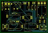
ive got a 2 layer pcb. ive added a ground plane to the bottom without a problem. it has been suggested that i add a copper pour to the top layer as well. just cant figure out if im doing it right. Do i assign a net like the previous? how do i set it to be on TOP?
Ive tried to add it without assigning a net but i get a report with an error "no area could be defined" something to that effect. sorry i closed the report. thought my noggin had some room left to remember a simple phrase. guess not. help if you can. thank you