Hello everyone,
I have been making some single sided PCB's over the last few months. However, I am experiences some difficulties. Sometimes the process seems to work fine, but sometimes the etching process eats away at my copper tracks, which makes the board unusable.
This is my set up:
- UV light box (megauk)
- Developer (Sodium hydroxide free) I use a concentration of 15g developer, to 800mL of water.
- Ferric Chloride etching crystals, I use a concentration of 250g, to 600mL of water.
- PCB photosensitive copper board
- Temperature. I do this process in my shed as electronics is just a hobby, temperature is usually between 10 and 20 degrees Celsius.
This is the process I use:
Create image:
Printed on heavy tracing paper using a laser printer, I print at least 600dpi. I try to configure the setting on the printer to print as black as possible, in the highest resolution.
Expose photosensitive PCB to UV light:
First of all I warm up the light box for 5min. I then place my PCB photosensitive side down on the image (so it is touching the toner side of the image). I then expose to UV light about 6min.
Develop image:
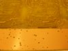
I place the PCB into a tray which contains the developer. It stays in there until I clearly see the image, the image usually changes from faint yellow to a brown colour. This usually takes about 10 seconds. I do not bother agitating the solution, as it seems to work fast anyway. I then rinse with water.
Etching:
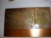
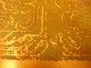
I then place my PCB into a tray containing my etchant. Usually it can take hours for all unwanted copper to be removed. Once removed I then rinse with water.
Now here is the confusing part.
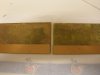
Last month I done this process with fresh etchant and developer, at first I did not get good results, my copper tracks seemed to etch too. Then after many, many tries, it started to work, and work for quite a few boards. When it works I acheieve good results, all tracks are perfect, even tiny ones.
This month I renewed the developer and etchant. I start to get my copper tracks etched again.
I have a feeling it could be the timing on my developing, but not sure. What do you think?, I would appreciate any help on this. It is driving me mad, is this process supposed to be simple?
What happens if a PCB is underdeveloped or overdeveloped?
Kind regards,
Jay
I have been making some single sided PCB's over the last few months. However, I am experiences some difficulties. Sometimes the process seems to work fine, but sometimes the etching process eats away at my copper tracks, which makes the board unusable.
This is my set up:
- UV light box (megauk)
- Developer (Sodium hydroxide free) I use a concentration of 15g developer, to 800mL of water.
- Ferric Chloride etching crystals, I use a concentration of 250g, to 600mL of water.
- PCB photosensitive copper board
- Temperature. I do this process in my shed as electronics is just a hobby, temperature is usually between 10 and 20 degrees Celsius.
This is the process I use:
Create image:
Printed on heavy tracing paper using a laser printer, I print at least 600dpi. I try to configure the setting on the printer to print as black as possible, in the highest resolution.
Expose photosensitive PCB to UV light:
First of all I warm up the light box for 5min. I then place my PCB photosensitive side down on the image (so it is touching the toner side of the image). I then expose to UV light about 6min.
Develop image:
I place the PCB into a tray which contains the developer. It stays in there until I clearly see the image, the image usually changes from faint yellow to a brown colour. This usually takes about 10 seconds. I do not bother agitating the solution, as it seems to work fast anyway. I then rinse with water.
Etching:
I then place my PCB into a tray containing my etchant. Usually it can take hours for all unwanted copper to be removed. Once removed I then rinse with water.
Now here is the confusing part.
Last month I done this process with fresh etchant and developer, at first I did not get good results, my copper tracks seemed to etch too. Then after many, many tries, it started to work, and work for quite a few boards. When it works I acheieve good results, all tracks are perfect, even tiny ones.
This month I renewed the developer and etchant. I start to get my copper tracks etched again.
I have a feeling it could be the timing on my developing, but not sure. What do you think?, I would appreciate any help on this. It is driving me mad, is this process supposed to be simple?
What happens if a PCB is underdeveloped or overdeveloped?
Kind regards,
Jay
")