Continue to Site

Welcome to our site!

Electro Tech is an online community (with over 170,000 members) who enjoy talking about and building electronic circuits, projects and gadgets. To participate you need to register. Registration is free. Click here to register now.

  • Welcome to our site! Electro Tech is an online community (with over 170,000 members) who enjoy talking about and building electronic circuits, projects and gadgets. To participate you need to register. Registration is free. Click here to register now.

Making a Bluetooth adapter for a Car Phone from the 90's

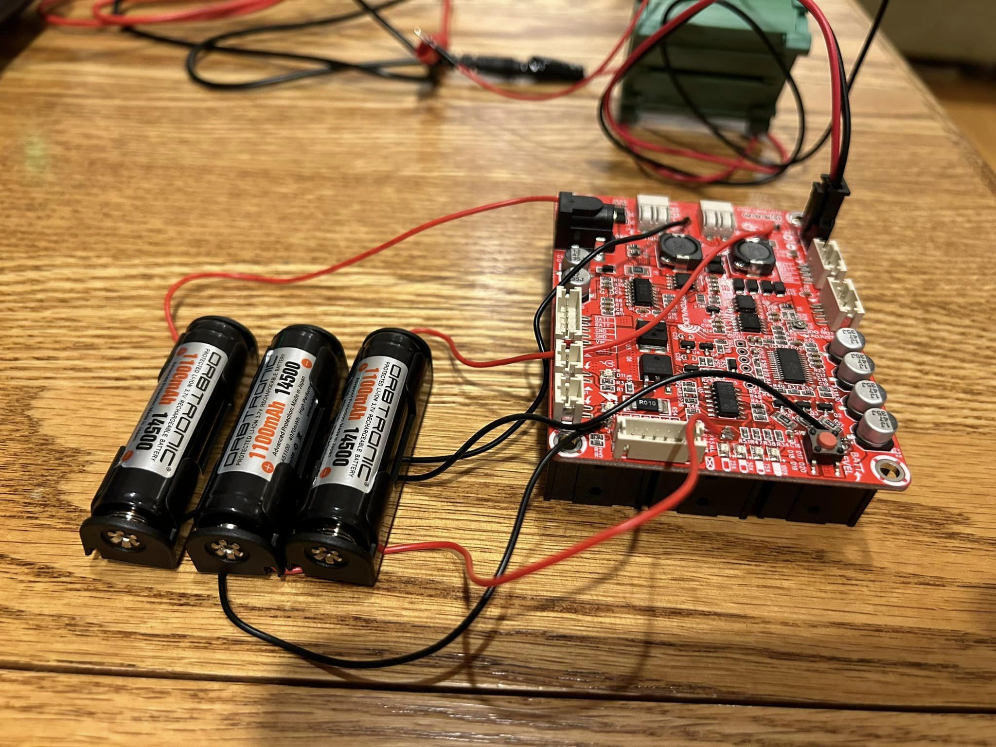
I received my AA-sized Li-ion cells and some battery holders with leads for testing. I soldered the AA battery holder leads to Dayton Audio LBB3v2 board while leaving the original 18650 size battery holders in place. This is just temporary for testing purposes.
1703731821261.png


These are 1100 mAh Orbtronic cells; the highest legit capacity cells I could find (there's plenty of fraudulent listings for various lower capacity cells claiming to be much higher 2500 mAh, etc.).

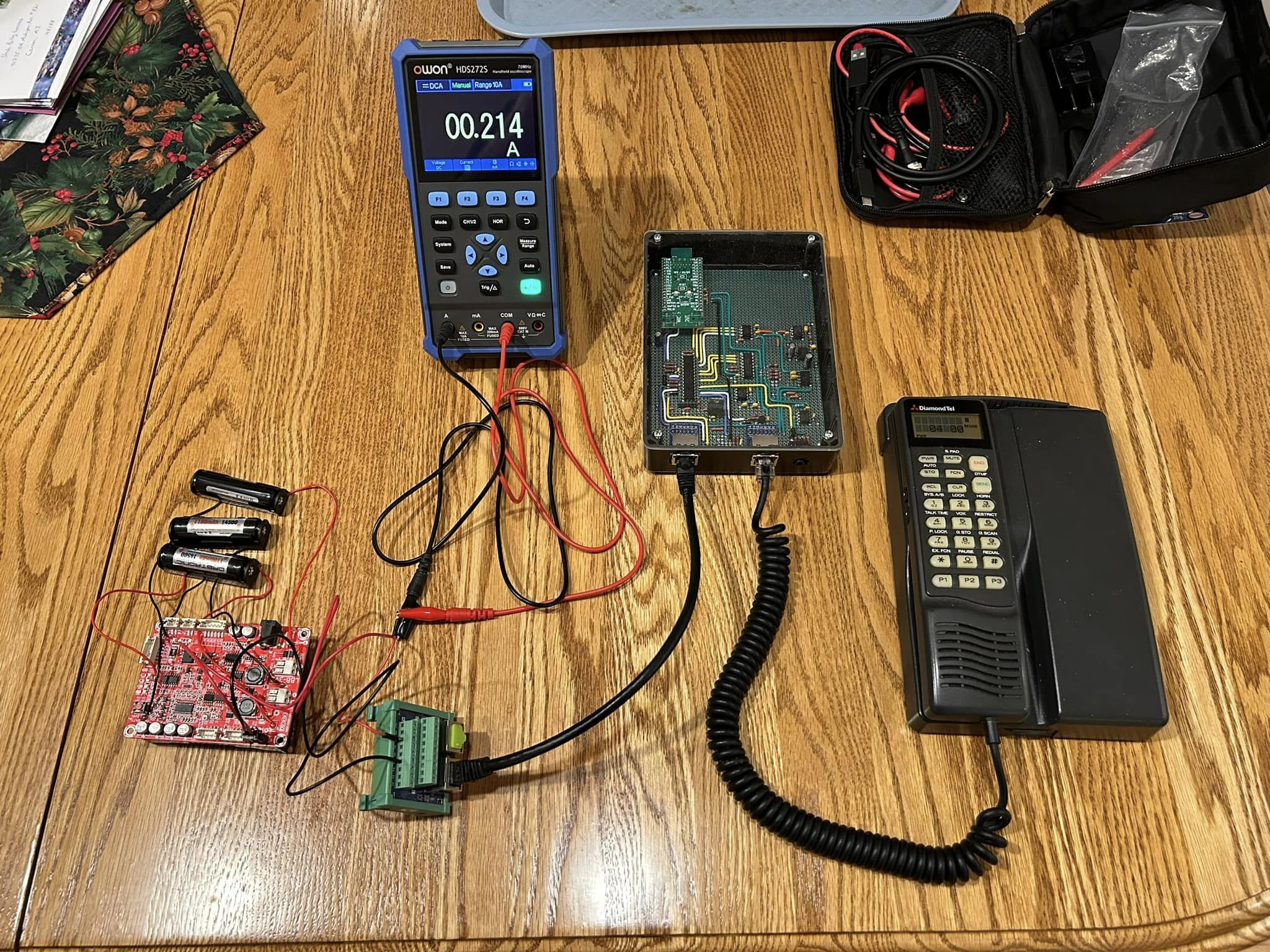
I'm definitely getting my money's worth out of the RJ45 breakout board I bought when first starting this project. This time I used it to provide power from the battery module directly to my Bluetooth adapter prototype, and also measure amp draw:
1703732122718.png


Here's some results (this is total amp draw of my circuit AND the car phone handset:
  • Idle, with handset backlight off, but with an active BT connection:
    • 55 mA
  • In a call, audio to ear speaker, music playing from the other end of the call, max volume:
    • ~170 mA average
  • In a call, audio to loudspeaker, music playing from the other end of the call, max volume:
    • ~215 mA average (I saw a peak of 225 mAh at a loud part of the song)

Assuming that about 90% of the Li-ion battery capacity with be practically "usable" (not sure if that's a good assumption or not), I should expect to see:
  • About 18 hours of "standby" (idle) time.
  • About 5.8 hours of "talk time" on the handset.
  • About 4.6 hours of "talk time" on speakerphone (although, you typically wouldn't have a an external mic handy for speakerphone use when carrying the phone around on battery power).

It's not a fair comparison, because I'm not powering a 3-watt 1G cellular radio, but here's the claimed specs from the original car phone user manual with its 1400 mAh NiCad battery pack:
  • About 16 hours "standby" time.
  • About 80 minutes "talk time" with the transceiver set to "low power" (probably only usable if you were in an area with strong signal).
  • About 50 minutes "talk time" with the transceiver set to "high power".

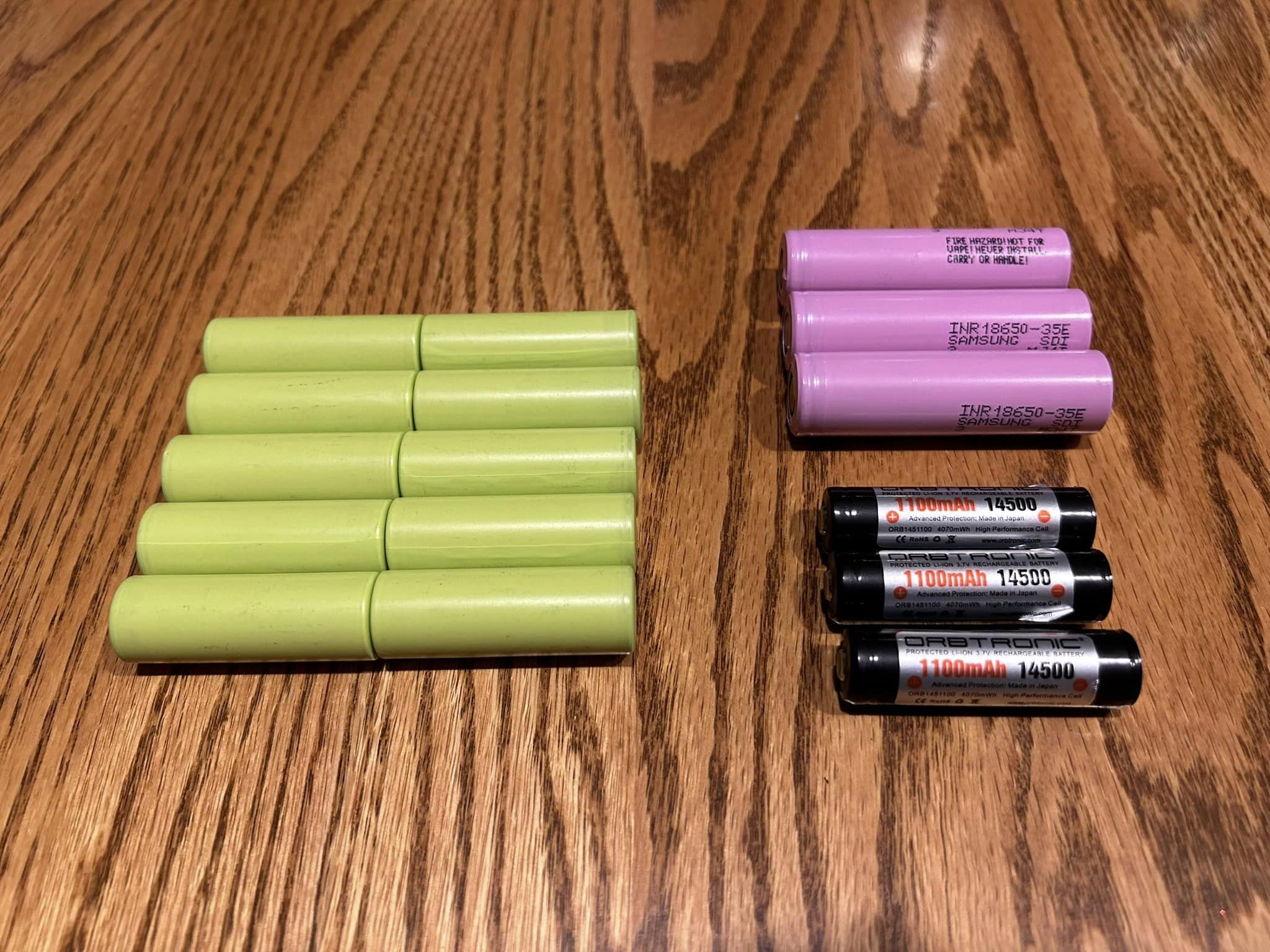
And just for fun, a side-by-side comparison of different battery cells:
1703733013190.png


  • Left: 10x "A" size 1.2V 1400 mAh NiCad cells used in the car phone's original battery pack.
  • Top Right: 3x "18650" size 3.7V 3500 mAh Li-ion cells that I bought for use with my Dayton Audio battery module, but they are too big for my project.
  • Bottom Right: 3x "14500" size ("AA") 3.7V 1100 mAh Li-ion cells that I'll be using.
 
Last edited:
I think I'm pretty happy with the PCB layout now:
  • I thickened up all of the audio tracks a bit and shifted some things around to route some digital tracks more nicely between the MCU, analog switch IC, and the digital potentiometer (see the 6 parallel tracks coming out of the upper right of the MCU).
  • I added helpful notes about connector pinouts, type of battery to use, and indicated where electrical tape should be added to the board to protect tracks from contact with dividers/structure of the metal case.
  • My mounting holes are now grounded so that the metal case will be grounded.
  • Ground fills are all "stitched" together with plenty of vias.

motherboard_pcb_top_half.PNG


motherboard_pcb_bottom_half.PNG


I printed the circuit board layout on card stock paper to test fit it in the transceiver case. My wife conveniently had a 3 mm hole punch in her crafting supplies, which is close enough for punching out the 3.2 mm mounting holes. I only had to make a few minor adjustments to a couple edges and mounting holes (0.5 mm was my largest adjustment), and now everything seems to fit and align nearly perfectly, with some slack in the slightly oversized mounting holes.


1703963839190.png


And finally, I discovered that KiCad's library of 3D parts models was missing the file for the battery holder. So I got the official 3D model from the battery holder manufacturer's website and got everything hooked up for a more complete 3D render of the board:


motherboard_pcb_3d_top.PNG


motherboard_pcb_3d_bottom.PNG


Now I need to get back to building my updated prototype of my initial plug-n-play design to verify my updated audio circuitry before committing to getting this board printed.
 
Last edited:
I completed the new version of my first plug-n-play prototype. The goals of this version were:
  • Go back to my original design of using a pair of INA105 precision unity gain op amps to produce the differential audio output and confirm that it eliminates the obnoxious digital noise from the handset UART communications.
    • Success! Noise eliminated.
  • Test with a stripped down BM62 Bluetooth chip breadboard adapter to verify that the absence of all the extra speaker/mic audio jack circuitry on the adapter will not affect performance of my circuit design.
    • Success! My circuit seems to perform just the same with the simplified adapter.
    • The only things mounted to the new BT module adapter board are the BT chip itself, 2 indicator LEDs, and the pin headers.
  • Try simplifying a few details.
    • Success! I was able to remove an unnecessary capacitor (still technically on the board in the photo, but not connected; I was testing both ways), an unnecessary voltage biasing connection and resistor on the analog switch IC, and change a capacitor value from 1uf to 0.1uf for consistency throughout the audio circuit.

First prototype on left. New prototype on right (note: the microphone jack broke off of the BT breadboard adapter on the left when I was installing/removing it multiple times for configuration updates):

1704575037875.png


I now have more confidence to move forward with the new PCB motherboard an Bluetooth daughterboard design.

And yes, I did try using both prototypes to make a call from one car phone to another car phone (I have many spare car phones). I ran into some interesting interference issues between the two Bluetooth modules. They seem both have the same Bluetooth MAC address, because my cell phone can't separately pair to each one. It thinks they are the same, even if they have different names. I need to look into this more, but so far have not been able to find any way to set the Bluetooth MAC address (also known as the BT_ADDR).

I also experienced a problem with microphone audio not working when answering an incoming call... sometimes. I first thought it was a problem with my new prototype, but then was able to reproduce it on the old prototype. When the problem happens, I'm able to "fix" it by either putting the call on hold than back off hold, or by putting the handset "on hook" then picking it back up (which triggers commands to the BT module to turn echo cancellation on for hands-free mode, then back off). So it seems to be a problem with the Bluetooth module itself that clears up after sending commands to the BT module that cause it to re-establish the audio connection, or make changes to audio processing options. My best guess at this point is maybe something about the timing of commands to answer the call vs command to change the echo cancellation setting, relative to when the call state actually changes... or something? I just need to play around with timing of my echo cancellation commands to test this hypothesis.
 
Last edited:
I modified my Dayton Audio LBB3v2 battery module so that it will fit in the car phone transceiver and connect to the JST-XH connectors I plan to use on my PCB.

Removing the battery holders from the board was a bit tricky because they are not just soldered, but also glued:

1704575875908.png


I added 3 wired connections with JST-XH connectors:

1704575926365.png


The 6-pin connector is for the external battery cells. One 2-pin connector is for external power input, using solid core 22-gauge wire so that the other ends of the wires can be inserted into the wago-like power input connector. The other 2-pin connector is for power output, soldered directly to the board where the larger black "high amp" power output connector was. Using the original power output connector as-is would not have fit inside of the transceiver.

Here's a preview of how it will sit on the PCB and connect to it:

1704576129849.png


And before I get the PCB printed and assembled, I want to test my power management circuitry and software (which I still need to write) on a breadboard. So I made a "battery pack" I can plug into the battery module, and a pigtail for connecting power output to a breadboard with solid core wire:

1704576358466.png


Battery holders are mounted to some scrap perfboard with double-sided tape (the thick squishy kind typically used for mounting electronic components in RC cars, etc.).
 
Last edited:
Success!

1704656730708.png


I was able to load firmware/configuration onto the Bluetooth chip with a USB adapter:

1704656795910.png


And I connected it to my prototype to confirm the audio and reset connections are fully functioning:

1704656890402.png


I only encountered one problem: I mis-labeled the dip switches! It caused some temporary confusion and panic while I was attempting to load configuration onto the Bluetooth chip and it wasn't working (because I had the dip switches set according to the incorrect labels).

I think I'm going to re-design this PCB with surface mount components to make the whole thing smaller, and to get some practice soldering those smaller components before I take on assembly of the motherboard. And it gives me a chance to correct the dip switch labels :).
 
Here's the new design of the Bluetooth module daughterboard, using surface mount components. I also eliminated the reset button because I can simply unplug the USB adapter and plug it back it in (reset via power cycling) between different stages of firmware/config updates. Or I could short the reset pin to the ground pin on the pin header with some scrap wire. Slightly less convenient, but less complexity on the PCB and no risk of the reset button somehow getting bumped when the board in use and mounted inside the car phone.

bm62_daughterboard_pcb.PNG


I also got a 3D model for the BM62 Bluetooth chip now :)

bm62_daughterboard_pcb_3d_top.PNG


bm62_daughterboard_pcb_3d_bottom.PNG


I also designed a few small pieces to help with positioning/mounting the connectors between the motherboard and the Bluetooth daughterboard wiring harness.

The original car phone has this pair of connectors to connect the transceiver with the battery and charging circuitry in the "transportable cover". I really wish I could find this exact pair of connectors, because that would make life much easier, but this seems to be long obsolete, or was a proprietary part made for Mitsubishi.

1704779283380.png


1704779327537.png


The connector on the "transportable cover" side has oversized mounting holes so it can shift and self-align as you install the cover. The socket on the transceiver is quite tall so that it protrudes out of a hole in the "lid" of the transceiver.

So I found an "elevated socket" part with very long "tails": https://www.mouser.com/datasheet/2/527/esq_th-1369982.pdf

You can actually order it with a stack of risers/spacers already installed, but they aren't any larger in dimension than the socket itself, so it seems like it would be very flimsy/unstable. So I'm getting small PCB parts printed to act as riser/spacers that have a larger base, similar to the original socket in the car phone transceiver:


socket_riser_pcb_3d_bare.PNG


socket_riser_pcb_3d.PNG


I think I'll need 4 or 5 of these to get the socket up to the necessary height.

Then for the mating connector, I'm trying this shrouded header, which will hopefully self-align well enough: https://www.mouser.com/datasheet/2/527/tss_th-2854503.pdf

The shroud is beveled to help with alignment, and the holes in the socket are also beveled to help guide the pins in. I designed a small PCB to mount this connector just like the original connector mounts, with oversized holes to allow it to shift around and align:

header_mount_pcb_3d_bare.PNG


header_mount_pcb_3d.PNG


I doubt it will work as smoothly as the original connectors, but I think it should work well enough.

I'm trying a different PCB prototype printing service this time: OSH Park

They have a smaller minimum quantity than DigiKey DKRed (3 vs 4), which I used for my first Bluetooth module PCB. I already priced out the much larger motherboard, and it will be $223 for 4 from DKRed, or $186 for 3 from OSH Park. Even though the per-board cost is lower with DKRed, I'd prefer lower overall cost at this point (I may never use more than 1 or 2 of these boards). So I'm taking this opportunity to give OSH Park a try with smaller/cheaper order.

I already like one major difference: OSH Park actually sends email notifications as your order progresses through the process (when it gets assigned to a "panel", when the panel "fills up" with orders and is sent out for manufacturing, etc.). They even tell you how many other orders are being printed on the same panel as yours. I presume I'll also get a notification when my order ships. DKRed did not provide ANY notifications of any kind, aside from the initial order confirmation. I just unexpectedly received my boards one day.

They also have two color options: Purple solder mask, or a black substrate with clear solder mask (so that all the copper traces are visible).
 
Last edited:
Why not use JLCPCB and get them with most components already fitted?
It's usually cheaper than buying the parts separately, from my experience?

eg. This is part of one of our prototypes, a four layer one, just as received:

JLC_Board_sm.jpg
 
Why not use JLCPCB and get them with most components already fitted?

Thanks for the suggestion. I will definitely be looking into that option for the motherboard. That would be great if I could get it cheaper and with all the surface mount components already soldered on. Might be worth the wait on shipping from China.
 
Thanks for the suggestion. I will definitely be looking into that option for the motherboard. That would be great if I could get it cheaper and with all the surface mount components already soldered on. Might be worth the wait on shipping from China.
As long as you don't mind paying for expensive (DHL) shipping then it usually takes about a week to the UK, but I've only ever ordered bare boards, I've never had any built up. However, I presume it doesn't take very long for them to assemble the boards?, so transport time is likely to be the biggest issue.
 
Looks like I can get 5 copies of my "motherboard" PCB partially assembled (all SMD capacitors and resistors, plus the 5V regulator IC) from JLCPCB for about $100 USD, shipped. The through-hole components are easy enough for me to take care of myself, and all the ICs (except the 5V regulator) are non-stocked.

I'll have to look more into the process of pre-ordering the non-stocked ICs so that they can also be included in assembly, but the MCU in particular is not available at all. JLC's part finder claims that it is no longer manufactured. That's strange, because Microchip's website doesn't say anything about the part being obsolete. It says they are in production and available to order.
 
It's working! Before committing to ordering circuit boards for my new car phone Bluetooth adapter design, I wanted to test the new power management circuitry and confirm that I could interface it with the microcontroller to make everything work as intended. So I built the new circuit design on a breadboard, minus all the audio circuitry (because that's not changing compared to my prototype that already works). I'm glad I did this, because I did discover a few problems with my circuit design and had to correct them.

1705345362456.png


This is now proof that I can successfully build a complete replacement for the original car phone's transceiver (and I already know I can fit it inside of the original car phone transceiver case).

Bottom right is the external power supply and vehicle ignition switch connection, with a toggle switch to simulate the ignition turning on/off.

The breadboard has some basic circuitry that allows the microcontroller to detect when external power is connected and when the ignition is on (using zener diodes to clamp the external voltage to <= 5V to be used as a digital input).

External power from the breadboard then connects to the battery power/charging module (top right; red circuit board) that manages charging the batteries and supplying ~12V back to the breadboard through another connector. A set of 3 li-ion rechargeable batteries is below the battery module.

The microcontroller has constant power so it can always be monitoring the handset power button, external power connection, vehicle ignition, and battery voltage. There's a pair of relays on the breadboard, about in the middle, that allows the microcontroller to be in control of turning on/off a 5V and 12V circuit that is used to power the rest of the circuit only when the phone should be "on": Bluetooth module (small red circuit board, bottom center), car phone handset, and eventually all the audio circuitry.

And finally, I had to update the software on the microcontroller to monitor all of these new inputs and turn everything on/off accordingly.

The handset's power button can turn the system on/off if it is either running on battery power, or external power is connected with the ignition on (can't turn the phone of if its installed in the car, but the car is off). Press and hold the PWR button for half a second to turn on. Press and hold for 1 second, then release, to turn off.

If external power is not connected, and the handset is "hung up"/"on hook", then the handset's backlight and audio will be turned off after 10 seconds of inactivity to conserve battery.

If the phone was turned on while external power was connected with the ignition on, then turning the ignition off will turn the phone off.

If the phone was turned off by the ignition, and external power has not since been disconnected, then turning the ignition back on will turn the phone back on.

I'm estimating battery level based on detected battery voltage to:
  • Display approx battery level on the handset when requested.
  • Report approx battery level back to the paired cell phone periodically so the cell phone can display it as a Bluetooth headset battery level.
  • Warn the user when battery level drops to ~5% (periodic beep and "LOW BATTERY" message on the handset).
  • Automatically power off when battery level gets too low (not yet implemented).
  • Refuse to power on if battery level is too low (not yet implemented).
 
Last edited:
I have a mix of software and hardware updates from the past week...

  • I implemented more functionality in software:
    • Rolling average of battery level readings to reduce "jitter".
    • Different slightly higher threshold for exiting "low battery" mode vs entering "low battery" mode to avoid bouncing back and forth.
    • Prevent the phone from being turned off while in a call.
      • If connected to external power and vehicle ignition is turned off mid-call, then the phone will automatically power off when the call ends or the Bluetooth connection is dropped.
      • This behavior can be disabled with a user preference configuration if you prefer to be able to turn the car phone off mid-call (which will transfer audio back to the modern cell phone).
    • Automatically power off when battery voltage drops to a minimum level (that is safely above the Dayton Audio battery module's low voltage cutoff).
      • And prevent attempts to power on if the battery voltage is too low.
    • I think the software will be pretty much ready to go by the time I receive and finish assembling PCBs :)
  • I had issues with the reed relay for the handset's 12v power supply sometimes sticking closed/on when turning it off. It would click open if I disconnected the handset's power supply wire (i.e., remove the load), then connect it again. It would also click open if I tapped it. I suspect there was some kind of voltage/current spike exceeding the "switching" limits relay as the switch was opening... maybe caused by the audio circuitry in the handset? The continuous current draw of the handset is well within both the continuous and switching limits for both amps and watts. I solved it by turning off all power-hungry features of the handset (backlight, all audio) then waiting a short delay before switching the relay off. The relay now reliably turns off immediately every time.
  • I found that my high-impedance voltage divider + op-amp buffer for providing ADC battery voltage input to the MCU was not really saving much power consumption compared to a simple lower impedance (< 10k ohm as per MCU specs). The op-amp draws about 1 mA, while a simple voltage divider is drawing about 1.5 mA. The op-amp also suffered some non-linearity when the signal approached Vdd. In hindsight, I should have been able to predict this by looking at the datasheet of the op-amp. I'm simplifying to just a voltage divider.
  • I struggled for a while to write/organize code in a way that I could reliably reset all important state when transitioning to a "powered off" state in preparation for the next power-on. I gave up and decided to just reboot/reset the MCU entirely when powering down, and have it enter a "powered off" state immediately (unless I have stored a flag in EEPROM signally to power on at startup; used in a few situations for a reboot sequence that is not a power-off).
  • I tried using the MCU's SLEEP mode when "powered off", but I can't figure it out. It always immediately wakes up. I've even tried disabling all unused peripherals and disabling interrupts for things that I don't want to wake the MCU. I have the WDT disabled. I only want my I/O pin "interrupt on change" to wake the MCU so that I can process the power button and ignition switch changes.
  • But I decided I don't care that much about true SLEEP mode if I can't figure it out. After disabling all peripherals I never use, and disabling some peripherals that are only used when powered on, my circuit (5V regulator, MCU, and voltage divider for battery voltage detect) is down to 8.3 mA when "off" with the MCU still running at full speed. I'm sure that's a horrifyingly inefficient pig by modern standards, but it's good enough for now.
    • Measured from an external power supply into the total system (with batteries and battery charging module, etc., with batteries fully charged), my project draws 43 mA when off, and the original car phone draws 159 mA when off. So it's already a huge improvement over the original and will have less parasitic draw on my car's battery when parked. I'd guess that the continuous trickle charging of the NiCad battery pack (to maintain its charge) is probably a major contributor to the original car phone's amp draw in this situation.

Other news:
  • My new Bluetooth module PCB and my small socket/header mounts/shims shipped today! (There was several day delay due to severe winter weather in the northwest of the US. They had about an inch of ice covering everything)
  • I started preparing to order the main "motherboard" through JLCPCB with all the surface-mount components assembled.
    • I had to pre-order several non-stocked components, and I had to user their "global sourcing" to order the MCU from RS Components.
  • One component I ordered through JLCPCB is estimated to arrive Feb 14, and I can't order the boards until the parts are in inventory, so I have plenty of time to go over my circuit design, PCB design, footprints, etc., to double-check correctness of everything and repeatedly find the "ugliest" part of my PCB layout and try to make it nicer.
    • I already found a few serious mistakes. I had a resister hooked up to the wrong input of an IC, I had the RX and TX pins of the handset connector mixed up, and the symbol/footprint I had imported into KiCad for the reed relay was incorrect! So now I need to go through and double-check all symbols and footprints against datasheets.
 
I think I'm approaching the "good enough" point with my PCB design and I need to stop endlessly fiddling with it and just hope for the best... or at least better than my perf-board prototype :).

I'm really limited by some physical constraints of the shape of the transceiver case, positions of connectors, and where I can place the Dayton Audio LBB3V2 battery module and the connectors to connect it to my board.

I just can't avoid having extremely long traces to connect external power supply voltage (bottom left connector: J1) to the battery module (one of the upper-left connectors: J4), then the from the battery module power output (another one of the top-left connectors: J5) down through all the various power supply components (5V regulator, relays for switching power, -5V supply, and +2.5V supply) and finally down to the components that need power. The switched 12V trace from one of the relays all the way down and across to the handset connector (J2) is particularly long. And so are all the traces for connecting the batteries to the battery module.

I did my best to try to limit the number and length of traces on the bottom side of the board
(blue) so that it can be mostly a ground place. And I tried to keep such traces oriented more "vertical" than "horizontal" to try to limit obstructions to a direct path from components back up to the ground pin of the battery board supply connector (the "source" of ground for the entire board). But it's quite a tangled puzzle of connections that need to be made between the components, and I can't seem to find a graceful way to provide power to all the components through that web of connections.


1706163422373.png


All of the power supply stuff (aside from batteries and the battery module) is neatly contained in this section of the board, which is also an isolated "walled off" portion of the transceiver case too:

1706162990041.png


This bottom half of the layout is where all the fun and mess happens.

1706162827001.png


1706165931167.png


1706166049406.png


1706166202330.png


I'm excited to get some of these boards in my hands and find out if they work and will fit in the transceiver case as intended. I expect this to happen around the end of February.
 
How did I miss this? I just realized I can clean these 3 traces up by changing the pin assignments on the MCU so they don't have to cross each other.

Screen Shot 2024-01-25 at 11.22.29 AM.png
 
I decided I don't care that much about true SLEEP mode if I can't figure it out. After disabling all peripherals I never use, and disabling some peripherals that are only used when powered on, my circuit (5V regulator, MCU, and voltage divider for battery voltage detect) is down to 8.3 mA when "off" with the MCU still running at full speed. I'm sure that's a horrifyingly inefficient pig by modern standards, but it's good enough for now.

I got the MCU to stay asleep! I ended up saving a copy of ALL interrupt enable registers, clearing them all out, then specifically enabling ONLY the pin IOC (interrupt on change). Now it stays asleep until I press the handset PWR button, connect/disconnect external power, or turn the vehicle ignition on/off. Upon waking, I restore all interrupt enable registers to the saved values. If conditions are not met to power on within 2 seconds, then I put it back to sleep.

After getting this working and disabling peripherals not needed during sleep, I'm down to 4.55 mA current draw when "off". Of that, 1.22 mA is the voltage divider used to drop the battery voltage down to a range that can be read by the MCU as an analog input for battery level detection, and the rest must be wasted energy from the linear 5V regulator.

I tried to measure amp draw from the output of the 5V regulator to my circuit when in sleep, and my meter must not be able to accurately read whatever tiny amount of current the MCU is drawing in sleep, because I actually got a small negative result.
Are you programming in assembler or C?, if you use C then all the interrupt saving issues are taken care of.

I do a LOT of low power PIC programming, and disabling the peripherals you aren't using seems to make sod all difference, as I've been there and done that :D

What 5V regulator are you using, if it's a 78L05 then it's quiescent current is quite high, where the MicroChip MCP1702-5002 was a quiescent current of only 2uA - plus it's LDO, and 250mA rather than 100mA.

Battery monitoring is an issue, but can easily taken care of by a buffer opamp (I use the MicroChip MCP6022), allowing the use of much higher value resistors in the potential divider, and you simply power the opamp a switched supply - or don't use the opamp, and use lower value resistors fed from the switched supply.

So basically, have the low power 5V regulator feeding the PIC, and then an FET switch feeding the 5V to everything else - switched ON and OFF by the PIC - so nothing else (including the voltage monitoring resistors) other than the PIC and the regulator are drawing any current. I use a small SM dual-FET to do the switching.

One point to watch is what peripherals are doing while the PIC is in sleep - if you're not careful things like serial ports can draw draw current out the pin while it's sleeping, to cure that, disable the serial port, and set the pin LOW.

Monitoring such low current is difficult, and I bought a 'Current Ranger' for that very purpose - even then it's not that easy, as the PIC wakes up and draws current briefly. For your regulator/potential divider measurement, simply unplug the PIC, and measure the current with no PIC in circuit :D I'm quite horrified by 1.22mA just for battery monitoring.

I've found it completely impossible to even approach the claimed power consumption, even if you're running nothing except a PIC, but I get over 5 year battery life with the techniques I use. According to larger manufacturers in the trade, as long as you can get below 100uA average consumption you're doing OK.
 

New Articles From Microcontroller Tips

Back
Top