Hi earckens,
If you mean connecting Vz to Ov, yes.
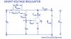
By the way, if you look at the schematic in post #20, you will see the constant current system rearranged, but that is not to detract from Les' excellent detective work.
")
You had better get back to your missus or all three of us will all be in trouble.

spec

") ), I think indeed you already had rearranged something to that effect back then if I remember well.. To bad I had overlooked.. sorry!
), I think indeed you already had rearranged something to that effect back then if I remember well.. To bad I had overlooked.. sorry!
 (but messing with a PDF in Photoshop is a bit demanding and I find it difficult analyzing the circuit when it does follow the layout rules- sorry earckens)