Continue to Site

Welcome to our site!

Electro Tech is an online community (with over 170,000 members) who enjoy talking about and building electronic circuits, projects and gadgets. To participate you need to register. Registration is free. Click here to register now.

  • Welcome to our site! Electro Tech is an online community (with over 170,000 members) who enjoy talking about and building electronic circuits, projects and gadgets. To participate you need to register. Registration is free. Click here to register now.

Learning 8051

Status
Not open for further replies.
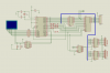
Attached is my 8051 development board with 32Kx8 SRAM 61256.

Where do the 3 wires on the SRAM ie. /OE, /WR & /CE go to?

Can I leave the /EA & /PSEN not connected? I know I need to put 10K pullup resistors on port 0. The schematic is done in a rush.

Allen

If you are using the external data buss to parse/fetch data from external RAM you won't need pull up resistors on P0. They have strong internal pull ups when used as the external front side bus.
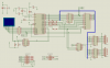
On the RAM -

/OE would go to the P3.7/RD pin on the 8051. This is the read strobe input.
/WE would go to the P3.6/WR pin on the 8051. This is the write strobe input.
/CE is typically used as a paging pin to lock the memory chip into a block of memory. This pin should go to P2.7/A15. This locks the memory chip into the 0x0000-0x7FFF region of memory space. Reads/writes to the 0x0000-0x7FFF will read/write to the memory chip while reads/writes to the 0x8000-0xFFFF region will do nothing unless some other piece of hardware is using that address space.

/EA = External Access. This pin must be tied to +Vcc if using the 8051's internal program memory
/PSEN = Program Store Enable. This is the read strobe when using external program ROM. It does not get used when using internal program memory and can be left disconnected.
 
That's very informative. And here is the updated schematic.

I added 2x 8 bit latches 74LS373 (I got plenty) as output ports for LCD and keypad. Can I use 74LS374 or 74LS323 8 bit F/F instead ?

Is there anything wrong with my reset circuit ? Do I need a reset button? As you see that I put in 16 jumpers on the Data and Address just in case I need to make use of port 0 and port 2.

Allen

[edit] oops I forgot to remove the pullup resistors.
 

Attachments

  • my 8051 dev board 2.PNG
    my 8051 dev board 2.PNG
    392.9 KB · Views: 2,685
Last edited:
The 74LS series is way outdated. I use the 74HC/HCT series, which are TTL level CMOS rather than bipolar, hence they consume less current than standard TTL devices.

I use the 74HC573, which is functionally identical to the 373, just with a more convenient pin out.

The 74LS323 is a shift register, not a latch.

The 74LS374 is basically the same as a 373, but the CP pin takes the place of the LE pin and it is edge triggered vice being level triggered like the 373. Seems like it would work, though I cannot say 100% since I've never tested it before.

The reset circuit on the 8051 is active high (backwards from PIC and AVR, which are active low reset). You have it tied high with a pull down capacitor. You should have a pull down resistor and an optional pull up capacitor. A 10uF cap from RST to +Vcc with a 10K resistor from RST to ground will provide a 100mS power on reset. Reset button is optional as well, but it must go between RST and +Vcc.
 
The 74LS series is way outdated. I use the 74HC/HCT series, which are TTL level CMOS rather than bipolar, hence they consume less current than standard TTL devices.

I use the 74HC573, which is functionally identical to the 373, just with a more convenient pin out.

Yes, but I dont have any HC573 left and I hate to order a few chips by mail order as they would charge postage/courier if I order <$50.

The 74LS323 is a shift register, not a latch.

Oops sorry, I forgot to check the datasheets.

The 74LS374 is basically the same as a 373, but the CP pin takes the place of the LE pin and it is edge triggered vice being level triggered like the 373. Seems like it would work, though I cannot say 100% since I've never tested it before.

Thanks, I'll try with a 374 and see if it works. Will report back if it doesnt.

The reset circuit on the 8051 is active high (backwards from PIC and AVR, which are active low reset). You have it tied high with a pull down capacitor. You should have a pull down resistor and an optional pull up capacitor. A 10uF cap from RST to +Vcc with a 10K resistor from RST to ground will provide a 100mS power on reset. Reset button is optional as well, but it must go between RST and +Vcc.

That's why I felt a little suspicious, but the sample files in my proteus was wired up like that so I just follow their mistakes and it seems to work just fine.

At the moment I am busy wiring my board and testing the programmer I bought from eBay. The programmer was meant for 89C51 using RS232 com port from PC. No sure if it would work with the 89S52 that I received recently. he wiring on the 7 segment sub board is the most difficult part. I have to solder all the wires on the back of the little PCB. The a-g segments of the 2-digit LED were not wired internally and I have to multiple them using short jumper wires which made the job tougher.

It would take a few days before I can test my program on the real hardware to see how it performs.

My next project is to add a 4x4 keypad and a LCD on port 2 & port 3. If possible on the external ports $8000 & $8001.

Is there a bootloader program for the 8051? If not, I am thinking of putting a small OS program in the 89S52 and test the program on external SRAM. Time to do some "movx" instructions. Of course the serial communication has to be working first & that's another project itself.

Allen
 
I attached my latest circuit for my 8051 dev board.

Here I have a couple of questions regarding the circuit.

1. What role does "RST" play in the ISP programming? Does it also supply +12V to 8952 during programming? If that's true, will the 10uF, 10K Power On Reset disturbs the programming of the chip?

2. If /EA is tied high, Could my external SRAM be able to run programs?

I also connected E3 of 74HC138 to A14 so only 0x8000-0xBFFF are used for I/O.

Allen
 

Attachments

  • my 8051 dev board 3.PNG
    my 8051 dev board 3.PNG
    141.8 KB · Views: 2,078
Last edited:
1. What role does "RST" play in the ISP programming? Does it also supply +12V to 8952 during programming? If that's true, will the 10uF, 10K Power On Reset disturbs the programming of the chip?

RST doesn't supply anything. It is an input pin. This pin should be externally pulled high (5V) when in programming mode. You would end up having to disconnect RST from the external cap/resistor and tie the pin to 5V with just an external pull up in the range of 4.7K - 10K when programming the chip.

Out of curiosity, what programming hardware are you using? I use the AT89ISP cable, which should be able to control the high/low setting of RST when in programming mode regardless of the external hardware.

2. If /EA is tied high, Could my external SRAM be used for running programs?

When /EA is tied high, external code execution only occurs when the internal program attempts to address a code memory address that is past the internal code space via acall, lcall, ajmp or ljmp. In the case of the 89S52, this would mean that the code would have to jump to a code memory address range of 0x2000-0xFFFF in order for external code execution to take place. Code execution on addresses 0x0000 - 0x1FFF would take place from internal memory.

However, when /EA is tied low, all code is executed from external memory.

I also connected E3 of 74HC138 to A14 so only 0x8000-0xBFFF are used for I/O.

Allen

A 74HC138 is a 3-8 address decoder. How it is meant to be used is to divide the external 64K of external RAM space into 8 blocks of 8K by connecting the A0-A2 pins of the 74HC138 to address pins A13-A15. /E1 and /E2 are usually tied low directly while E3 is tied high directly. Then, the Y0-Y7 pins are used to drive the /CE pins of each memory chip (or other external hardware) low when each block of 8K xRAM memory space is addressed -

0x0000 - 0x1FFF = Y0 Low
0x2000 - 0x3FFF = Y1 Low
0x4000 - 0x5FFF = Y2 Low
0x6000 - 0x7FFF = Y3 Low
0x8000 - 0x9FFF = Y4 Low
0xA000 - 0xBFFF = Y5 Low
0xC000 - 0xDFFF = Y6 Low
0xE000 - 0xFFFF = Y7 Low

This would allow there to be 8 RAM chips of 8KB each on the external buss. Or you can have a single 8K memory chip and other multiplexed hardware on the bus by using buffer chips with either an output enable or a chip enable pin, then use the Y0 - Y7 pins to assign the other external hardware to an 8K block of external RAM.

Make sense?
 
Last edited:
Jon Wilder said:
Out of curiosity, what programming hardware are you using? I use the AT89ISP cable, which should be able to control the high/low setting of RST when in programming mode regardless of the external hardware.

the programmer that I have is attached for your ref. It was designed for AVR and some of the internet software that I found might support the programming of 89S52.

Failing to program my 89S52 than I would have to construct the programmer from here:

**broken link removed**

OR

**broken link removed**

Jon Wilder said:
A 74HC138 is a 3-8 address decoder. How it is meant to be used is to divide the external 64K of external RAM space into 8 blocks of 8K by connecting the A0-A2 pins of the 74HC138 to address pins A13-A15. /E1 and /E2 are usually tied low directly while E3 is tied high directly. Then, the Y0-Y7 pins are used to drive the /CE pins of each memory chip (or other external hardware) low when each block of 8K xRAM memory space is addressed -

0x0000 - 0x1FFF = Y0 Low
0x2000 - 0x3FFF = Y1 Low
0x4000 - 0x5FFF = Y2 Low
0x6000 - 0x7FFF = Y3 Low
0x8000 - 0x9FFF = Y4 Low
0xA000 - 0xBFFF = Y5 Low
0xC000 - 0xDFFF = Y6 Low
0xE000 - 0xFFFF = Y7 Low

This would allow there to be 8 RAM chips of 8KB each on the external buss. Or you can have a single 8K memory chip and other multiplexed hardware on the bus by using buffer chips with either an output enable or a chip enable pin, then use the Y0 - Y7 pins to assign the other external hardware to an 8K block of external RAM.

Make sense?

Yes, that makes perfect sense. I will consider that decoding scheme but then I would need a 4-input AND gate to 'and' the outputs of Y1 - Y4 for my 32K SRAM. The schematic would look something like this...... Looks like I need another sub-board for the decoders.:rolleyes:

Allen
 

Attachments

  • AVR-USBasp User Manual.pdf
    43 KB · Views: 508
  • my 8051 dev board DECODER.PNG
    my 8051 dev board DECODER.PNG
    21 KB · Views: 1,170
Last edited:
The AT89ISP is available from my local Farnell. I am not sure if it is worth to invest $40 for it as I know I can build one that works almost the same.

Here is an update of my 8051 dev board and the AVR programmer that I have.

Allen
 

Attachments

  • DSC00338_rs.JPG
    DSC00338_rs.JPG
    499.8 KB · Views: 657
  • DSC00339_RS2.JPG
    DSC00339_RS2.JPG
    101.1 KB · Views: 526
Last edited:
Actually...you could just not use outputs Y1-Y4 and tie the CE pin on the SRAM to address pin A15 on the 89S52. This will make it so that only addresses 0x0000-0x7FFF access the RAM (A15 low). Anything above that will drive /CE high via address pin A15, thereby free'ing up addresses 0x8000-0xFFFF to be split into 8K blocks via outputs Y5-Y8 on the 74HC138 (A15 high). That will save you some hardware gating.
 
I just bumped into that thread when I'm also playing with the AT89S52 on a rainy night. That's a very informative thread.

Since I don't have a USBASP programmer, I temporarily used my old 20-year old parallel printer cable and turned it into an ISP with a 74hc244 soldered. I used the programmer software from http://dybkowski.net/content/en/node/15.

Also, I used the SDCC compiler since I don't feel like downloading Keil (trial version) as my connection slows down nowadays.

I might try to interface it with a bigger SRAM I have lying in the drawer if I have more time. :)
 
Hello well I must say this is very useful topic for me.
as I am a beginer in microcontroller.
I hope it will be fine if I can extract something from here and can ask doubt if any?
absf : Can you give me the tutorial which Ian posted..
 
Hello well I must say this is very useful topic for me.
as I am a beginer in microcontroller.
I hope it will be fine if I can extract something from here and can ask doubt if any?
absf : Can you give me the tutorial which Ian posted..
Which tutorial??? I haven't posted any tutorials on the 8051 yet!!!! I'm going to as soon as I have finished them...
 
Hello well I must say this is very useful topic for me.
as I am a beginer in microcontroller.
I hope it will be fine if I can extract something from here and can ask doubt if any?
absf : Can you give me the tutorial which Ian posted..

The tutorial Ian posted was on Post #37 here

https://www.electro-tech-online.com...-microcontroller-need-your-help.133921/page-2

There is a goode 8051 IDE that I used for developing the 8051 software in ASM in post #4.

HTH

Allen
 
Status
Not open for further replies.

Latest threads

New Articles From Microcontroller Tips

Back
Top