absf
Active Member
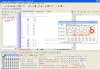
I have started my own thread for learning the 8051 using the "MCU 8051 IDE" and ISIS. Instead of sharing a thread with ikelectro, I think this is better so it won't interfere with his progress...
Anyway I have ordered the 89S52 chips from Element 14, and they should be arriving next week if they have the stock. Meanwhile I would just play with the IDE and Proteus.
After reading the instructions set from PDF file uploaded by Ian. I was able to understand a little bit more on the "Addressing Modes"
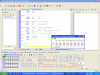
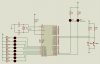
Here's my first program on stepping the LEDs on Port1 from right to left..
Ian, is there any particular reason that you left a hole between 0000h to 0030h?
Allen
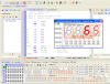
Anyway I have ordered the 89S52 chips from Element 14, and they should be arriving next week if they have the stock. Meanwhile I would just play with the IDE and Proteus.
After reading the instructions set from PDF file uploaded by Ian. I was able to understand a little bit more on the "Addressing Modes"
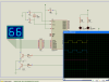
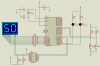
Here's my first program on stepping the LEDs on Port1 from right to left..
Code:
 ORG 0000H
SJMP START
ORG 30H

start:
setb p2.1 ;SW1 = 1
setb p2.0 ;SW2 = 1

init: mov A,#01 ;Acc =b00000001
mov r0,8 ;r0 is a counter
cpl A ;complement Acc

while: mov p1,A ;LIGHT UP RIGHTMOST LED
acall delay ;FOR A WHILE
rl A ;shift to next LED on the left
djnz r0,while ;done 8 LED?
sjmp init ;start another round
delay:
mov r1,#40h
loop: djnz r1,loop
ret
endIan, is there any particular reason that you left a hole between 0000h to 0030h?
Allen
Attachments
Last edited:

")