ljcox:
Thanks for your diagrams, this is helping me understand active high and active low a little better... not an easy concept to grasp. You got any literature on this topic specifically? You're welcome. I have a paper written in 1969 that explains the concept. I'll find it later, scan and post. Did you read the "gating paper" that I attached?
My understanding though (ACTIVE LOW) is when current flows to the input of the IC, the output is going to be '0', but when the current is interrupted to the input of the IC, the output will then become '1'. (like a normally closed relay, when receiving current, the remote circuit is open, when the current is stopped to the coil of the relay then is normally closed and '1'.) Is this correct for Active low? Obviously Active HIgh is opposite.
Don't consider the input current. The input voltage is the important issue. For CMOS, the input resistance is very high so there is virtually no input current. Also, it is less confusing to use High and Low rather than 1 & 0 since in positive logic, H = 1 & L = 0, but in negative logic, H = 0 & L = 1. High and Low refer to the voltages not the logical values, ie. H & L are physical attributes of the IC.
The Active High (AH) and Active Low (AL) refers to the input conditions to make a gate "active" For example, an AND gate is active when both inputs are High. ie. a H and a H makes the output H. So the output is AH, ie. the output condition when the gate is "active".
A NAND gate is "active" when the inputs are H & H but the output is L. So the output is AL. Read my gating paper for all the combinations.
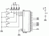
I've attached two pics of the joystick opened up (yes its definately USB, not serial or anything like that)... but I really cant see any IC's.... there are two black roundish epoxy blobs... but they really do look too small to have a chip... although I could be wrong considering the size of IC's these days.
As others have said, the blobs are ICs.
I see from your diagram that in the active high circuit you use 74hc02 and the active low you use the 74hc32, and I see on the PDF of these chips that they either have active high/low outputs respectively... thats easy... what I dont understand though is that you are using the same IC 74hc08 for both active high and active low circuits.... and that IC seems to be active high, so surely it wont work correctly on the active low circuit?
Read the gating paper. It shows how eg. an OR gate can be used to do either the OR function or the AND function. In the former case, the inputs are AH and the output is AH, but in the latter, the inputs are AL and the output is AL. Look at the truth table. H or H gives a H at the output. But when the inputs are L & L the output is L, hence it can be used to do the AND function.
philba:
Thank you for your very easy to understand drawing, I'm very grateful for your efforts!
Question: What exactly are the resistors needed for, I see you're dropping the voltage before the inputs to the IC, is 5v too much??? How does this work? The resistors are "pull up" resistors. The input to a gate must be either H or L. If you use a switch (as you are) to generate the input signal, you need a pull up resistor, otherwise, the IC won't see any change of voltage when the switch is thrown from open to closed or from closed to open. With the PU resistor, the input is "pulled" to +5V when the switch is open and "pulled Low when it is closed.
Question2: you've drawn switches S1-S4 with another little symbol above the actual switch symbol, the little squiggle and the sideways 'T' (sorry for the stupid description)... what does that represent? Sorry for all the stupid questions!!!
Question3: You have used the 74151N IC, how on earth do you know what IC to look for out of the many thousands they make??! ALso, the solution to my problem requires AND's and NAND's/NOR's according to ljcox and my friends logic diagram. Does this IC have these? I looked at the datasheet online and my God, I was very confused by the linework logic diagram within the IC... I dont know how you know what outputs to pick....
Look at the truth table in the data sheet.
ljcox: I take it the HEX inverted IC will convert active High/Low inputs to its opposite logic?