GromTag
Active Member
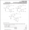
Regards to device by manufacturer that may differ by each 555 timer made. This is an block Diagram, there should be numerous types online to check in regards to design all tho not all manufacturers may display the actual block diagram accordingly or even be close in design to this depiction.
This example and info based on what I have observed via the LM555 Timer that I acquired for an project.
The VCC pin 8 within devices applicable range, depending on the voltage will change the resistor divider within the chip resulting in a different voltage requirement for the trigger via the Comparator #1.
The resistor divider depending on voltage at VCC will also determine the control voltage at
pin 5 Comparator #2 inverting input.
Comparator #1 function.
Internal resistor divider voltage from main supply sets the non inverting input of comparator #1.
The trigger pin 2 produces an inverted operation of comparator #1 upon the trigger going from high to low from being above the required voltage level based on supply voltage to an low causes the comparator #1 output to go from low to high during the trigger being briefly held low starting the set function of thr flip flop. And at the same time the flip flop deactivated the discharge transistor allowing the capacitor to charge slowly from the resistors current limiting.
This is of a few issues that can cause the output to stay on if the trigger is held low continuously.
The comparator #1 output stays high holding the set function of the flip flop. The flip flop reset pin 4 going low can override this. However if the trigger is still low when reset is taken back to high, the output will switch on again and stay on for the capacitor charge time to continuous. If the trigger is taken high after this, the remaining capacitor charge up time if any left is used then output switch off.
Comparator #2.
Internal resistor divider sets the voltage at comparator #2 inverting pin control voltage.
Comparator #2 pin 5 control voltage in monostable mode requires the capacitor to stabilize the voltage reference to comparator #2 inverting input.
The voltage into pin 6 from the charging capacitor must exceed pin 5 control voltage to result an change in comparator #2 output within the IC. The charge of timing capacitor causes the non inverting pin to go above the inverting pin resulting in an low to high output from comparator #2. This causes an reset signal to the internal flip flop. Output switches off and the discharge transistor switches on via an likely inverted Q feature from the flip flop.
The discharge transistor holds the capacitor low continuously until the trigger is taken from high to momentary low again.
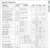
Electrical Characteristics included for an reference only.
And as stated an leaking capacitor would never charge up to the required voltage, this can be determined via testing pin 5 voltage and then after some time elapsed after triggering the timer to start check the voltage on the timing capacitor to see if it is near or above, if above and the device is still on then something elsewhere is going wrong with the IC.
This example and info based on what I have observed via the LM555 Timer that I acquired for an project.
The VCC pin 8 within devices applicable range, depending on the voltage will change the resistor divider within the chip resulting in a different voltage requirement for the trigger via the Comparator #1.
The resistor divider depending on voltage at VCC will also determine the control voltage at
pin 5 Comparator #2 inverting input.
Comparator #1 function.
Internal resistor divider voltage from main supply sets the non inverting input of comparator #1.
The trigger pin 2 produces an inverted operation of comparator #1 upon the trigger going from high to low from being above the required voltage level based on supply voltage to an low causes the comparator #1 output to go from low to high during the trigger being briefly held low starting the set function of thr flip flop. And at the same time the flip flop deactivated the discharge transistor allowing the capacitor to charge slowly from the resistors current limiting.
This is of a few issues that can cause the output to stay on if the trigger is held low continuously.
The comparator #1 output stays high holding the set function of the flip flop. The flip flop reset pin 4 going low can override this. However if the trigger is still low when reset is taken back to high, the output will switch on again and stay on for the capacitor charge time to continuous. If the trigger is taken high after this, the remaining capacitor charge up time if any left is used then output switch off.
Comparator #2.
Internal resistor divider sets the voltage at comparator #2 inverting pin control voltage.
Comparator #2 pin 5 control voltage in monostable mode requires the capacitor to stabilize the voltage reference to comparator #2 inverting input.
:External note:
The control voltage can be altered only to produce other functions as to
why it is available as an externally interactive pin.
However that applies a different direction and will not be discussed
as I am not aware of those functions as I only acquired
an 555 for the monostable basic function.
Online data is available for astable and numerous other
configurations that result in alterations to the pin 5 and others set up.
The voltage into pin 6 from the charging capacitor must exceed pin 5 control voltage to result an change in comparator #2 output within the IC. The charge of timing capacitor causes the non inverting pin to go above the inverting pin resulting in an low to high output from comparator #2. This causes an reset signal to the internal flip flop. Output switches off and the discharge transistor switches on via an likely inverted Q feature from the flip flop.
The discharge transistor holds the capacitor low continuously until the trigger is taken from high to momentary low again.
Electrical Characteristics included for an reference only.
And as stated an leaking capacitor would never charge up to the required voltage, this can be determined via testing pin 5 voltage and then after some time elapsed after triggering the timer to start check the voltage on the timing capacitor to see if it is near or above, if above and the device is still on then something elsewhere is going wrong with the IC.

![IMG_4225[1].JPG](/data/attachments/94/94975-51fd0c4d7a13b56f715d2fa823e74c82.jpg?hash=Uf0MTXoTtW)


")