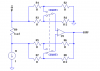
On the CD4053, what voltages are you using for VDD (pin 16), VSS (pin 8), and VEE (pin 7)?
The VSS and VEE of CD4053 are tied to Ground.The VDD=+12v
You need to show polarities of measured voltages. VCAL should be negative.
I think i had already done that..please see my text below the schematic.(had forgotten to give the negative sign)
Looking at U4 as an example, you have something wrong with either the op amp, grounding, or your measurement equipment/technique. Is this built on a PC board? Do you have a ground plane? Can you post a photo of the circuit board?
This is built on a PC board.I haven't brought my Digital camera with me and my phones camera is a meagre 1MP.I will post the Artwork and the layout some time later in the day.
I measure this with a good calibrated Voltmeter.I don't have a ground plane as such ,but i have connected the grounds from each op-amp individually to the common ground track
One more thing i noticed:
I was measuring the voltages at VDIFF & VCAL by providing voltages from a preset to DAC-REF SET and CURRENT SET i/ps.When i connected a MCU to this setup there are severe disturbances

First,the VDIFF at the same currents measures 300-400mV.
The DAC (12 bit) of the MCU cannot distinguish the smallest voltage scaled on a value 0xFFF=3.3v (or rather,is highly non-linear).I am thinking of creating a table of all the values needed and scale them manually.
I see a lot of problems here and the delivery date for this is the 10th of Jan.Lets hope all works out fine
")
Thanks for your time
EDIT: Changed 4053 supplies to VEE=-12v ,VSS=Ground and observed.No change!!!Attached PCB details

 )
)
 that brought a smile..