Continue to Site

Welcome to our site!

Electro Tech is an online community (with over 170,000 members) who enjoy talking about and building electronic circuits, projects and gadgets. To participate you need to register. Registration is free. Click here to register now.

  • Welcome to our site! Electro Tech is an online community (with over 170,000 members) who enjoy talking about and building electronic circuits, projects and gadgets. To participate you need to register. Registration is free. Click here to register now.

Grid Tie Inverter Schematic 2.0

Status
Not open for further replies.
oh they cut out the url sencce it was my first post oh well here are the part list they say
Part list:

4- Alternistors: Part# 511-BTA25-600BW*
4- Diodes: (at least 600V 0.1A). To make sure all parts are approved and UL certified we use a couple of Bridge Rectifiers part#512-GBPC1506*
1- Large capacitor or capacitor bank: We use 2 400V 5 UF.
Some heavy gauge wire and quick connector (from local hardware/electrical store
1- piece of 6" x 8" aluminum plate as heat sink.
2 fuse holders and 220V 30Amp fuses*. (4 fuses are better)
Terminal block for DC and AC 110V wall plug/receptacle.
Some screws, small bolts, and nuts.
Even its back side looked complex but it is exactly the same as the schematic above. It's front is much clearer and simpler.
The rated wattage of the device are defined by the ohm law W=V *I, in this case it the alternistors are rated at 600V and 25Amp; assuming that the the capacitor(s) is large enough.
 
Not a clue.

Fist off How do you get the DC to pass through the capacitor on the negative line? :confused:
 
what do i know though i barely know anything about ac and waves i need a osiliscope. im just interested in the triacs and why cant they be used?
 
If you managed to find that schematic with Google searches you can certainly find some good info on SCR and Triacs and how they work along with loads of info on AC wave theory.

Not to be rude but if you don't know much about AC power and basic semiconductor switching devices you are way over your head being in this thread and attempting to deal with this subject.
 
Grid Tie Inverter idea

Hi all,
I've followed this and the first one long thread about Grid Tie Inverter, because I'm a power electronic lover I've read a lot of IEEE paper on the subject in order to gain some detailed knowledge on this type of DC-AC conversion system.
As a first attempt I've simulated a simple schematic based on a single stage conversion system able to work with a single PV panel (my goal will be build a low power inverter and mount it directly on the back side of the solar panel).

This first schematic I've sketched is a full bridge topology with a line frequency transformer for safety reason, actually I'm try to build a didactical prototype, is not my interest to go into the commercial field, anyway is not difficult avoid the line transformer by using a boost stage between the PV panel and the output Full Bridge (this also avoid the core saturation issue detailed below into this post).

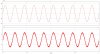
Here in attachement the converter schematic as I've draw and simulated inside P S I M and the image taken from the signal waveform.

The two block named MPPT and MONITOR implement respectively the MPPT algorith and the starting and functional sequence of the inverter operation from the power on to the steady state behaviour (this block was written in C language).

The panel choosed and modeled was a Inventux X3-115 (115 W, VMPP=125 V, IMPP=0.92 A, datasheet attached), the reason to use a high-voltage panel is to keep the current on the DC side of the inverter at a reasonable level, with this setup at the nominal 230 V grid voltage (rms value) the peak of the current trough the filter inductor was approximatevely equal to 3 A.

Actually this schematic is working correctly trough the simulation stage, may be into the future I'll build a real prototype.

The Power Factor from the simulation is equal to 0.967, this is due to the current loop control (the modeled sensor is a ACS712ELCTR-05B-T from Allegro). By using the current control approach the output current can track the sinusoidal reference which came directly by the PLL (in this way we can be sure about the grid current synchronization) and multiplied by a factor which came from the output of the MPPT algorithm. The used MPPT algorithm is a P&O and is able to track the MPP point from 200 W/m^2 to 1000 W/m^2 irradiation into the valid grid voltage range (here assumed from 195 V up to 264 V, all value is intended as RMS).

Conclusion
-------------
The only drawback about this schematic is that we've a transformer drived like a push-pull topology then we have to be sure about the flux inside it in order to avoid the transformer core saturation phenomena and this is the principal issue for a real and practical implementation of this schematic. A way to avoid this may be control the filter inductor current, in this way we can check about every DC current component that may be keep the transformer core into the saturation region. Of course in this simulation there is no matter about this trouble, but is a real problem and this is the reason because the Push-Pull converter topology is best controlled by using the Current-Mode control instead the simple Voltage Mode Control. Further step may be then avoid the line frequency transformer and study a transformerless stage, but here arise some other trouble due to the parasitic capacitance of the PV panel but this is another thing, actually I'm thinking to reason only with transformer based tolopolgy mainly for safety reason.

Further analysis
-------------------
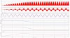
Anyway this is a simple first type approach, in these days I've also reverse engineered a commercial inverter and found in it a very simple schematic based around a push-pull topology controlled with averaged current mode by a simple UCC2806, now I'm going to simulate it by using directly the component value from the converter but I think there is some issue into the controller modelling into the simulator. Just to give some anticipation the UCC2806 control the current trough the push-pull MOSFET in order to following a full-wave rectificated sinusoidal shaped current reference. Due to this current control the current trough the primary of the high-frequency transformer should have a rectificated sinusoidal shaped structure and also the secondary current must following this shape. On the secodary side of the transformer we've a full bridge rectifier followed by a filter inductor (3.3 mH) and a filter capacitor (2.2 uF) and then the output line commutade MOSFET bridge that connect the inverter to the grid line. In other word the output bridge is self commutated by the grid in order to split the current into a positive and negative cycle at every grid cycle.
There is also two identical push-pull stage, for 230 V setup the two secondary circuit was put in series and for 120 V in parallel, more simple solution to have a multivoltage inverter able to work to all the grid voltage available into the word (the setup is made by configurable switch).
Regarding this topology I think this can be view as a current-fed grid commutated inverter switching at twice the grid frequency (attached IEEE paper figure 2a, page 783).

The end for now
--------------------
Remember that all is just for passion and not for commercial purpose!

I Hope to have made a little contribute to this thread in order to get more discussion from a lot of member inside this nice forum. I love to know other people with my passion and talking about this amazing stuff.

Thanks.

Regards
Powermos
 

Attachments

  • Powermos GTI V1.0.pdf
    66.9 KB · Views: 1,510
  • Signal-Simulation.jpg
    Signal-Simulation.jpg
    403.1 KB · Views: 1,158
  • Signal-Simulation-Detail.jpg
    Signal-Simulation-Detail.jpg
    204.9 KB · Views: 1,224
  • Inventux_X3_Datenblatt_EN_V0002.pdf
    1.8 MB · Views: 1,286
  • paper-Power Inverter Topologies for Photovoltaic Modules – A Review.pdf
    363.3 KB · Views: 1,798
Last edited:
Let me be the first to say thank you for a well presented addition to this thread!
 
Back Panel Mount Grid Tie Inverter (may be the future ?)

Dear all,
here below I like to present another topology well suited for single panel mounting and able to manage small power up to 200 - 300 W, this type of solution is usually classified as micro-inverter grid connected solution.

Advantage of a such type of solution is that the low-cost inverter will be mount directly on the back side of the solar panel. This short the cable length needed to connect the panel with the inverter compared to a centralized solution.
Also using the local inverter on the solar panel allow some flexibility because I've just to put the power cord of the inverter into one home plug to inject power as needed without the need to install a fixed plant on the roof.
Of course everyone have different need and request but I like to present also this solution for people that need to inject small power into the house grid in order to save some money, e.g. when in summer we start to use refrigerator. Of course the solution is convenient only if the overall cost of the single microinverter is small compared the number of inverter we need respect a centralized solution.

Anyway a part of particulary use I think that also study small inverter is useful to gain some knowledge on this very amazing field of power electronics. I love power electronics!!!!

As usual you can find in attachement the schematic that I've drawn to perform the numerical simulation (P S I M) and the most significative waveform taken from the simulation output, also I've attached the reference paper where interesting people can study in a more deeper way the presented topology. Into the original paper simulation was carried on by PSPICE programs but there is no reference about the simulation schematic then I've rewritten it for P S I M, another simulation tool in order to check if my result was in agreement with the ones into the original paper.
Also into the schematic I've set some detail about the analog circuitry used to sense the grid voltage and to sense the solar panel voltage and current (this last trough a low cost shunt but to save some power loss we can also use Hall sensor like the ACS family from Allegro which is also a low cost solution). Grid voltage sensing is did in a not isolated way (PAY ATTENTION TO THIS) with a low cost operational amplifier. Regarding the control (see the section PWM Generator into the bottom side of the attched PDF schematic) there is a subcractor of 2.5 V (to avoid the 2.5V continuos introduced by the Grid Sensing circuitry) then there is a block that make the full wave rectification of the input waveform (may be build with a couple of simple operational amplifier) and then there is a multiplier. Regarding the multiplier there is several low cost analog multiplier into the market (SO8 package), the other input of the multiplier into the simulation was set as a fixed value of 2V, into the real life this input should be connected to the MPPT stage in order to modulate the peak value of the rectified sinewave and the achieve the desired output power level from the inverter. Again, interesting reader can study the attached paper to gain lot of useful information on this topology.

Main difference of this setup compared the previous one that I've posted (Post#47) is that there is no need to sense the output current of the converter, the only current sensor is on the solar panel side (I've also to say that literature have been proposed also sensorless solution to avoid the PV current sensor or the PV voltage measurement, but I think that this issues are more attractive just for accademic talking than practical approach, this is of course my personal thinking).

The behaviour of the converter is then more simple and well described into the attached paper, the most important things is that the Flyback have to work always in DCM (Discontinuous Conduction Mode fixed switching frequency) or in BCM (Border mode, at the boundary between DCM and CCM with variable switching frequency) and never goes into the CCM (Continuous Conduction Mode).

I've to mention also that IEEE paper used to perform the simulation is freely downlodable from this link:

h t t p : // www . calpoly . edu/~taufik/inverter/paper8.pdf

Hope this stuff can be of some interest.

Bye for now
Powermos
 

Attachments

  • Flyback-GTI-Simulation-Schematic.pdf
    68.8 KB · Views: 1,127
  • Flyback-GTI-Simulation-Diagrams.jpg
    Flyback-GTI-Simulation-Diagrams.jpg
    335.3 KB · Views: 1,624
  • paper8.pdf
    569.3 KB · Views: 1,052
Last edited:
Flyback Grid-Tie design for 160W 35V solar panel module

Regarding a solar panel with PMP=160W and VMP=35 V I've recalculated the inverter parameter, into the attached schematic I've also drawn the circutry used to shape the rectified main reference voltage before feed this voltage to the analog multiplier used to set the output power.

Parameters for the solar module used into the simulation are reported below:

- VOC=42.80 V
- ISC = 5.15 A
- VMP = 34.9 V
- IMP = 4.60 A

Parameter for main is 230 V rms with frequency of 50 Hz.

As usual simulation schematic and signal waveform is attached.

IMPORTANT NOTE!!!!
Also remember that all this stuff is only for personal study and not for build a real prototype and connect it to the main grid because all the prototype must have on board a anti-islandig device and also must be certified to comply with the regional mains rules!

Best regards
Powermos
 

Attachments

  • Flyback-160W-35V-Solar-Module-Grid-Tie-Schematic.pdf
    81.4 KB · Views: 1,104
  • Flyback-160W-35V-Solar-Module-Grid-Tie-Schematic-Waveform.jpg
    Flyback-160W-35V-Solar-Module-Grid-Tie-Schematic-Waveform.jpg
    186 KB · Views: 1,961
Flyback Grid-Tie design for 160W 35V solar panel module - a personal revisitation

Dear all,
basing on previous post topology we can understand that the diode and MOSFET build on every secondary of the Flyback coupled inductor act as a simple unfolding stage then we can change it to another equivalent one based on the full bridge topology. Reason to did this change is to reduce the voltage stress on the secondary MOSFET and also to simplify the building of the Flyback transformer. In this way the transformer is a standard one with one primary winding and one secondary winding, this also have a goal to reduce the leakage inductance between the secondary winding and the primary winding and this is more simple to build in a home made fashion than a double secondary windings type.

Voltage stress in each MOSFET of the full bridge is the half of the previous section then a lower BVDSS voltage MOSFET can be used with the advantage that also the rdson is lower than a MOSFET rated for a greater BVDSS voltage.

I've to admit that this is a my personal elaboration of the IEEE paper schematic and may be useful to make a semplification into the prototype without the need to ask manufacturer for a custom wirewound transfomer that may be expensive.

As usual in attachement you can find the new schematic and the simulation result which is identical to the previous schematic based on the center tapped windings.

Best regards.
Powermos
 

Attachments

  • Flyback Grid Tie_Schematic.pdf
    68.8 KB · Views: 1,116
  • Flyback Grid Tie_Simulation.jpg
    Flyback Grid Tie_Simulation.jpg
    194.7 KB · Views: 1,048
  • Flyback Grid Tie-Center-Tapped-Schematic.pdf
    84.6 KB · Views: 974
  • Flyback Grid Tie-Center-Tapped-Simulation.jpg
    Flyback Grid Tie-Center-Tapped-Simulation.jpg
    204.1 KB · Views: 1,514
Explain for Flyback Grid-Tie design for 160W 35V solar panel module

I have a question about the output transformer 29//58. (schematic without center pont)
What the voltages should be and the power for 35V at position VA?

Also the points IPVUP and VPVUP for sensing the input current & voltage, what do they control?

Thank you in advance,
Giannis
 
Dear Giannis,
first of all thank you for your interest in this topic, you're the first after some time from my first post.

Before goes into the details I like to know some info from you.

Do you have built this prototipe or are just investigating for future implementation? What is your knowledge into the power electronics field?

Regarding the voltage at point VA I've designed this circuit able to work with a single panel with 35 V at MPP and a maximum of 160 W, but be careful if you like to build a real circuit about the transformer construction. Actually I'm doing some other deep analysis about voltage stress on the switching elements and current, also I've to conclude that to gain better result the only choice is build the custom transformer by some specialized manufacturer (if you did deep analysis for power around 160 W the peak current trough the primary winding is very high around 20 A and then need a very carefully construction of the transformer, leakage has to be keep as lower as you can).

About IPVUP e VPVUP this should be used to perform the MPPT algorithm calculation (e.g. with a microcontroller and then feed the AD inputs with this two signals).

Also keep in mind that the circuit schematic I've post is just a conceptual one, you've to use suitable driver and logic gating to drive the unfolding bridge and the main switch then the final circuit will be sligthy different than the used into the simulation for this obvious reason, but the value of the main elements is equal to the one that you can look into the simulation schematic.

Hope in some feedback from you.

I'll for sure build the prototipe in order to test the behaviour into the real world.

Regards
Pow
 
Last edited:
This is an excellent thread, thanks to everyone who has contributed; I'm learning a lot from it.

The main grid tie inverter schematic posted looks a bit over engineered (which is not a bad thing but complicated for a newbie like myself). I want to take a stab at building one and came across this one: https://solar.smps.us/grid-tie-inverter-schematic.html << is is there a major deficiency with this circuit?
 
Well for one no control or synchronizing circuits are shown in that link which is what my circuit here shows and why you find it over engineered.

If you are looking for bare bones functional but uncontrolled and don't care about efficiency or safety the 'Grid Tie Inverter schematic' thread has one. All it requires is two transformers, two resistors, two transistors, and a diode to work.
 
Pretty much dead now. Married, good paying job, working on building a house, that sort of stuff.

Not much justifiable time to play/experiment with AE any more. :p
 
I did this in the simulator and it seems to work.
What do you think,
what is your opinion for it ??


Well my opinion is that its overly complicated to doing such a simple function. I don't see the opto isolation as being necessary and the two diodes on the legs of the of the primary on the output transformer are completely unnecessary as well.
 
Status
Not open for further replies.

Latest threads

New Articles From Microcontroller Tips

Back
Top