Continue to Site

Welcome to our site!

Electro Tech is an online community (with over 170,000 members) who enjoy talking about and building electronic circuits, projects and gadgets. To participate you need to register. Registration is free. Click here to register now.

  • Welcome to our site! Electro Tech is an online community (with over 170,000 members) who enjoy talking about and building electronic circuits, projects and gadgets. To participate you need to register. Registration is free. Click here to register now.

Emitter resistor.

Status
Not open for further replies.

alphacat

New Member
Hey,
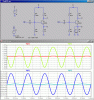
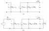
I learned about integrating an emitter resistor into a CE amplifier in order to have the transconductance gain (Gm) less depended on the ambient temperature (and also to increase Rin and Rout of the amplifier).

But on the other hand, such integration causes the gain (Gm) to be less than unity:
Gm turns to be gm / (1 + gm*RE), when originally it was equal gm.
Moreover, if RE is large enough so 1 << gm*RE, then Gm turns to be 1/RE (which creates a very large attenuation).

So what is the advantage in adding such resistor if it causes the amplifier to attenuate the input signal?
 
Last edited:
In a common-emitter amplifier, the gain is ~ Rload/Re, where Rload is the resistor between collector and Vcc, and if Re is not bypassed at signal frequencies. The usual practice is to put in an Re for bias/op point stability, but to bypass it at signal frequencies with a suitable capacitor so as to keep the signal gain up.
 

Attachments

  • CE.gif
    CE.gif
    52.1 KB · Views: 330
Last edited:
Please let me refer to RLoad as Rc (which is how its usually called).
Usually, Rload is the resistor which is DC coupled, so only the ac signal will reach it (RL in the attached image).

How did you conclude that the gain of a CE amplifer is RC / RE?

For the intrinsic amplifier (circuit 'a'), the gain is gm,
and for the loaded amplifier (circuit 'b'), if we assume impedance matching (Rout >> RL, Rin >> Rs), then the gain remains gm.

--
If you wonder how i concluded the gain of the intrinsic amplifier is gm, then when finding transcoductance gain, the output is shorted.
bjt-jpg.32030
 

Attachments

  • BJT.JPG
    BJT.JPG
    20.6 KB · Views: 1,080
Last edited:
Look at my previous posting again.
 
Hey,

Thanks for the great simulation.

Lets focus please on the non-bypassed emitter circuit (the left one).
I estimate Vout (Vc1) to be 0.1V * sin(ωt), according to the graph.
Now:
vin = 10mV * sin(ωt).
iout = vout / Rc = [ 0.1V * sin(ωt) ] / 10kΩ = 0.01mV * sin(ωt).
(vin, iout and vout are small signals, ac signals only).

Therefore: Gm = iout / vin = 1mS (S = 1/Ω).

Thats the attenuation i was talking about.

Its interesting:
gm = IC / vth = [(VCC - VC) / RC] / 25mV = 26.4mS (I assumed T to be at room temperature, therefore vth ≈ 25mV).
gm*RE = 26.4 >> 1.
Therfore: Gm ≈ 1/RE = 1mS, which is exactly the result i received above.
 
Last edited:
Oh, I think i understand my problem.

I was comparing Volts to Amperes, which i guess wasnt quite correct.
So what is the concept behind transconductance, if you cant compare between Volts and Amperes?
 
Transconductance is a wonderful tool for exploring theoretical nuances, but in real BJT design examples we use beta. That is, we use an approximation of beta, since actual production devices may, in practice, span half a decade. We use HFE for the static operating point, and Hfe for the signal gain.

And even if we know Hfe to six digits, we don't usually use a whole digit. (if given 477.2, I would design for 200 to 700).
 
HFE is DC current gain and hfe is AC current gain. They have nothing to do with voltage gain.

Voltage gain is the collector resistor in parallel with the load resistor or impedance, divided by the transistor's internal emitter resistance in series with the unbypassed external emitter resistor.
 
Could you tell me please,
βF is hFE,
and βo is hfe?

In the literature, they always use βo and βF, and in all examples that i saw there, βo was always equal to βF.
 
I have never heard of Beta-F and I have never heard of Beta-o.

hFE is DC current gain.
hfe is AC current gain.
Current gain is beta.
 
Thanks.

Is it common in datasheet to present hfe?
In most datasheets i always saw that they presented hFE (which they indeed call DC Current Gain), but i dont think i saw any data regarding hfe.

Besides, the AC signal only rides on the DC operating point (without changing it), so i figured that the AC current gain would be equal to the DC current gain.
In spice, i receievd a good proximity between IC/IB and ic/ib (when simulating a CE amplifier).
 
Last edited:
The datasheet for the 2N3904 transistor shows the hfe beginning at 1MHz.
The datasheet for the BC548 transistor shows its hfe at 1kHz.
The low frequency current gain is a little more than their DC current gain.
 
Thank you a lot.

Its good to obsreve it at last.
Does this difference between hFE and hfe come from the existance of junction capacitors and parasite capacitors?

When analyzing amplifiers, I usually ignore them and perhaps that was the reason why I concluded that hfe equals hFE.
 
Last edited:
Status
Not open for further replies.

Latest threads

New Articles From Microcontroller Tips

Back
Top