Continue to Site

Welcome to our site!

Electro Tech is an online community (with over 170,000 members) who enjoy talking about and building electronic circuits, projects and gadgets. To participate you need to register. Registration is free. Click here to register now.

  • Welcome to our site! Electro Tech is an online community (with over 170,000 members) who enjoy talking about and building electronic circuits, projects and gadgets. To participate you need to register. Registration is free. Click here to register now.

Eagle Jumpers

Status
Not open for further replies.

Gayan Soyza

Active Member
I have done a nice eagle schematic.

In schematic capture when doing the PCB there are some wires you cannot ROUTE anymore because they will overlap each other.

What you all doing for this UNROUTED wires? How do you place jumpers or pads for them?
 

Attachments

  • Jumpers.PNG
    Jumpers.PNG
    5.6 KB · Views: 1,319
Last edited:
Hi Gayan,

first you should try to optimize component placing. This will allow for more bottom layer traces. If there are still unrouted traces manually route on the bottom and then switch to top. Continue routing on top until you get to a point to finish the trace on the bottom layer. The lop layer trace should be a straight line for a straight piece of wire to use for a jump.

If you want to make the PCB yourself just omit the top layer and make it single sided. If you turn the design into a PCB manufacturer's you should get rid of top layer traces - otherwise he'll make a double sided PCB.

In that case ripup the top trace with an unbroken connection between vias (air wire with same net name). Use layer21 (component) and draw a straight line between those vias to remind you there is a jump when placing the components. If possible also name them on the PCB like "BR1" (BR=German abbreviation for jump or bridge)

About like this: (attachment)

Regards

Hans
 

Attachments

  • jumps-1.jpg
    jumps-1.jpg
    31 KB · Views: 1,229
EDIT: This assumes you want to etch your own PCB>

Layout the board as if it were two sided but etch only the bottom. After etching jumpers on the top side will solder to the vias on the bottom.

The attachment is not a great layout but it does a good job of illustrating what to do. It shows the top layer in red. Each red trace becomes a jumper.

It also shows that you can run traces between pads but it requires good etching to make it work.

3v0


I have done a nice eagle schematic.

In schematic capture when doing the PCB there are some wires you cannot ROUTE anymore because they will overlap each other.

What you all doing for this UNROUTED wires? How do you place jumpers or pads for them?
 

Attachments

  • PIC_18P_ROBOT_SS_1B.pdf
    16.6 KB · Views: 567
Last edited:
Hi Hans thanks for your idea.

My PCB is single sided & its making by myself at home.

In that unrouted wires how do you place two pads for a jumper?

Do I need to place pads in the schematic?If I place pads in the schematic my nice schematic is getting ugly :(
 
I have done a nice eagle schematic.

In schematic capture when doing the PCB there are some wires you cannot ROUTE anymore because they will overlap each other.

What you all doing for this UNROUTED wires? How do you place jumpers or pads for them?
Use wirepad?
 
Hi 3v0 thanks for your help also.

Same question from you also.

When routing the boad it doesn't support any pads but it support to place VIA's in the board editor.

So both of you telling me to place VIA's for each unrouted wires?
 
Last edited:
Yes.

While routing a wire, hold down the shift key and left-click the mouse. This will produce a via with copper on both sides of the PCB. Route right over the intersecting wires, then shift-left-click again will make a 2nd via. Finsh the trace. Then go back and do a change-layer to move the trace between the vias to the top side of the PCB.

If you want you can switch layers while routing but it is easier to explain the other way.

HTH

Hi 3v0 thats a very nice shortcut.Thats what I need.I have placed jumpers in my PCB using this method.

I must make sure turn on the VIA layer before doing this method.

Thanks 3V0 & Hans for your help.
 
Consistency Check

Hi AtomSoft thats a nice video thanks for your help.

New Problem

I was doing a schematic capture.When I finished 75% of the PCB I added new components to the Schematic.I got this message "No Forward&Back Annotation will be performed!- Parts missing in the Board".

After looking at the help file there was something called "Consistency Check"

The newly added components are not displaying in the board.ERC gives that message.I don't like to manually place the parts to the board either.

So I drawed the board again from the beginning.

Does anybody knows about "Consistency Check"
 
Hi Gayan,

the jumps in that post were vias. The difference between a via and a pad is this: A via is automatically generated changing layers when routing. A pad is component and consists of a symbol and a package.

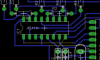
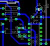
Now please take a look both, the schematic and the PCB-layout. The schematic contains four invisible pads, all connected to ground. (Just because I wanted it that way for demonstration purposes.)

Does it look ugly? :)

The layout could of course be done using a single layer board by placing the components another way. However if you are forced for some reason to place the I/O pads on top of the circuit you'll be confronted with a pretty wierd ground trace.

Pads in a schematic are treated like components. They must be connected. (otherwise the ERC will fail.) :(

There is more than one advantage to using pads instead of vias: First, ripup stops at the pad, while it might also delete a "valuable" via. Secondly, you can move the pad all over your PCB and it is still connected (to bee seen by the air wire). Drop it where ever you want and route the trace between two pads using the top layer or omit routing and draw a layer21 line between those pads as a reminder for a physical jump.

Here is an easy way to make "jump-vias". :D

Create a new library called pads.

- make a package using the desired pad diameter, shape and drill size. (The
- ones used in the example are exactly the same as IC-pins (1.6002mm dia,
- 0.8128mm drill size, shape octagon = standard Eagle usage for IC -
- packages). Number the pad or omit numbering

- make a symbol using pin length point, select "visible" - off. Number the pin
- or omit numbering. Don't use any text. When finished all you should have on
- screen is a green circle.

- create a device using symbol and package. Connect - and you're done

To use the "invisible" pin (pad) in the schematic switch to "Display" --> "pins". Grab a suitable pin out the libary and place it on the desired net. It connects automatically, so you won't have to worry about deleting and redrawing the net.

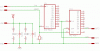
The sample circuit has no practical use. It was made for demonstration purposes only.

Regards

Hans
 

Attachments

  • JUMPS-2-SCH.gif
    JUMPS-2-SCH.gif
    10.7 KB · Views: 424
  • JUMPS-2.jpg
    JUMPS-2.jpg
    39.6 KB · Views: 436
Hey Gyan to avoid "No Forward&Back Annotation will be performed!- Parts missing in the Board" allways keep both schematic and PCB windows open. This will make shure that any new components or changing components will be done on both ;)

Good luck
 
Hi Hans

Thanks for your wonderful explanation.It clearly explains whats the different between a PAD & a VIA.Thanks for that.

I'll try to add some invisible pads like you described.

Hi Kryten

There was some mismanaged in my eagle project files.Something happened when taking backups & replacing the files.Thats why "No Forward&Back Annotation will be performed!"
message comes.Anyway I redraw it again.

After finished I'll show what I did, it has hell of a jumpers :D
 
Last edited:
The thing was in my project directory if I create a project as "New Timer" then it saves files like this------>schematic = New Timer.sch & Board = New Timer.brd

But see my attachment it creates lots of duplicate files.Sometimes I'm deleting this files may be that cause to pop up that error message.
 

Attachments

  • ProjectT1.JPG
    ProjectT1.JPG
    38.2 KB · Views: 308
As I see it a via is only used becaused it is needed to make the route. It makes sense have via's go away when you rip up a trace.

In general a pad connects to a part or wire so it makes sense that they be persistant.

I understand you dislike for the current way ripup works. Perhaps that should be addressed in Eagle. Maybe have ripup stop at vias unless you hold the sift key down or similar.

3v0

There is more than one advantage to using pads instead of vias: First, ripup stops at the pad, while it might also delete a "valuable" via. Secondly, you can move the pad all over your PCB and it is still connected (to bee seen by the air wire). Drop it where ever you want and route the trace between two pads using the top layer or omit routing and draw a layer21 line between those pads as a reminder for a physical jump.... Hans
 
Hi Gayan,

to regain the full files (schematic and board) copy the latest backup files, e.g. timer.s#9 and timer.b#9 in a different folder. Then rename them for the suffix "sch" and "brd".

When loading the schematic the consistancy check should be alright unless you goofed already there. If schematic and board are consistant you just have to take care of the latest changes of your design - instead of redrawing the whole thing. :D

Hans

BTW, the idea using hidden pins in a schematic was "born" when I talked about a simple copy protection in another thread. VCC and ground traces are predestined for that purpose. If somebody spots the hidden pins (pads or invisible pads with a diameter of 0.01mm :)) in the schematic and erases them he'll be in trouble with e.g. unconnected supply pins. One or two unconnected power pins on a PCB will certainly cause headaches when trouble shooting. :D
 
Hi thanks for bot of you.I must take of those files after.& need to care of latest changes as well.

One more question.

Whats the grid size you all using for the board & for the Schematic?

When creating custom parts whats the grid size you all selecting?
 
Status
Not open for further replies.

Latest threads

New Articles From Microcontroller Tips

Back
Top