Hi,
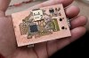
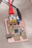
Well, I have finally got round to making my first double sided PCB using press'n'peel paper, its a small USB blaster clone, 2 x 1". I have read about aligning the p'n'p sheets, and taping them together to form a 'pocket', then sliding the substrate inside, and ironing. I did it by having two alignment holes on the top and bottom prints, and drilling through the PCB, then stapling both designs onto the PCB through thoses holes. No perfect, but not bad. All my vias lined up well enough.
Whilst I was doing it, I suddenly realised it would probably be far easier to simply etch two single sided boards, drill a couple of holes in them for alignment, then glue them together with epoxy, before drilling the rest. With 0.8mm (1/32") thickness board it should end up as standard 1.6mm thickness. Alignment should be pretty much perfect, since they are aligned 'after' etching using the existing drilled pads for alignment. A couple of vero pins, some epoxy and a vice/press, and it should work out.
It may sound like a lot of work, but dealing with 0.8mm board has its advantages, cutting/milling becomes a whole lot easier for a start.
I just wondered if anyone has done this before? of course there are no plated through holes (made my own copperset bails for that) but I have perfected the p'n'p method for 0.5mm pitch IC's so I'm looking for more ways to improve things.
Blueteeth.
Last edited: