hello,
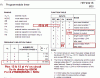
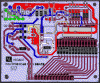
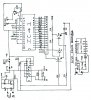
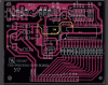
i have brought a kit of "digital alaram clock".i soldered by my self and it is working properly.i have to submit it in my college.but i dont know how it is working.because what schemetic diagram is there is very confusing.there are two IC's IC2 is CD4541 and IC1 is LM8560.one crystal (of 3.278 MHz)is connected to IC2.but there is not a singal connection which is supplying clock pulse or any type of pulse to IC1.whereas IC1 is clock cum alaram manager cum BCD to 7-segment converter cum 7segment driver,and v all know that clock IC need 1Hz or any type of pulse(which is not provided),then how the IC2 know when to increment the logic state or at what interval it has to give "COLON OUT".please write me an detailed working of this circuit if possible.i can provide u any material u want for proper understanding.i m attaching schemetic diag.,datasheet of both the ics and PCB LAYOUT of both Cu and component side.thanks
i have brought a kit of "digital alaram clock".i soldered by my self and it is working properly.i have to submit it in my college.but i dont know how it is working.because what schemetic diagram is there is very confusing.there are two IC's IC2 is CD4541 and IC1 is LM8560.one crystal (of 3.278 MHz)is connected to IC2.but there is not a singal connection which is supplying clock pulse or any type of pulse to IC1.whereas IC1 is clock cum alaram manager cum BCD to 7-segment converter cum 7segment driver,and v all know that clock IC need 1Hz or any type of pulse(which is not provided),then how the IC2 know when to increment the logic state or at what interval it has to give "COLON OUT".please write me an detailed working of this circuit if possible.i can provide u any material u want for proper understanding.i m attaching schemetic diag.,datasheet of both the ics and PCB LAYOUT of both Cu and component side.thanks
Attachments
Last edited:
")