Continue to Site

Welcome to our site!

Electro Tech is an online community (with over 170,000 members) who enjoy talking about and building electronic circuits, projects and gadgets. To participate you need to register. Registration is free. Click here to register now.

  • Welcome to our site! Electro Tech is an online community (with over 170,000 members) who enjoy talking about and building electronic circuits, projects and gadgets. To participate you need to register. Registration is free. Click here to register now.

DC-DC Buck Converter

Status
Not open for further replies.
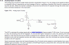
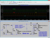
there's an article explaining the I/O speeds on a different mcu basis -- but we can predict the input rate being apx 1 x sys clk from Figues 10-3 & 10-4 -- that incase there is some ideal sync. between sys-clk and incoming digital signal otherwise it's variable 1 to 2 sys-clk.-s e.g. at 20MHz you can read in at predicted average 14Msps or at least 10Msps - - - - that if you use external comparator to compare V.out V.set or incase of external ADC // assuming 4-bit parallel input (is supported by port masked input instruction ????????) // the 12 bit DAC can be fetched at 3MHz - versus - 1 bit comparator at 10MHz . . . . . . . . . rserving some time to do internal lookup we assume 300k / 1MHz MOS-Fet control rate - - - 3 or 1 µs "sys don't care" free wheeling - - - whatever the timing - the current limit for inductor+mosfet should be another external device sending it's "triggered" status to mcu

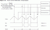
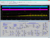
shortly -- without looking the code yet - but only the schematic - we can speculate the system being robust and not very flexy . . . unless the pwm modules have their own controllers and setting the pwm index does some miracles here ??? -- at max. clk/2⁸ (78.1 kHz) or clk/2⁹ (39.1 kHz) PWM cycle ??? -- related https://microchipdeveloper.com/8bit:10bitpwm
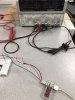
 

Attachments

  • Fig-11-08.gif
    Fig-11-08.gif
    18.2 KB · Views: 146
  • Fig-11-09.gif
    Fig-11-09.gif
    15.8 KB · Views: 147
status ::
// it seems that the PWM setup is highly ??? flexible (Tbl-12-03) but there is only one poor app example(was not searched ↓1-st **↓)/spec(was not found) ??? they must had a target design or a set of when developing the '13'25'45'85 chips - can't find any ???
http://www.instructables.com/id/DIY-BuckBoost-Converter-Flyback/
http://www.microchip.com/wwwproducts/en/ATtiny85
>> AVR PWM lit. ::
http://www.newbiehack.com/MicrocontrollerControlAHobbyServo.aspx
**broken link removed**
** http://www.atmel.com/images/atmel-42183-design-a-buck-converter-with-xmega-e_ap-note_at04204.pdf
http://www.ijareeie.com/upload/2014/may/7_Fuzzy_Logic.pdf
** http://www.avrfreaks.net/forum/resolved-attiny85-error-pll-high-speed-pwm
 

Attachments

  • Chp-17-08.gif
    Chp-17-08.gif
    21.9 KB · Views: 155
  • Fig-21-07.gif
    Fig-21-07.gif
    29.8 KB · Views: 158
  • Tbl-12-03.gif
    Tbl-12-03.gif
    18.6 KB · Views: 146
there is not much to do to get the required package of relevant data together - but as i in near future likely will not use that particular product - you can complete it and on your own ((moreover when the the share of my own free time input here is complicated by a nation based discrimination from the u.s. forum moderator itself . . . i'm not supposed to fight the windmills here or in anywhere else))

i haven't completed working through the references about ATTiny MCU your circuit uses

i suggest you do it yourself or email the instructables source of the circuit to find out the AD input and PWM output timings involved
PS! also inquire about the initial tune to operation procedure as you have 2 . . .actually 3 inputs
  1. +5V external reference as i get it
  2. the resistor divider
  3. the dc/dc step down voltage scaled by op amp -- what it's dynamic range and other characteristics should be in particular ???
if you know the timing and correct operating mode setup you can further work out the possible modifications to mosfet drive and inductor to enable your target 1.5A output
 
(though it seems faster is to find a random 12V AC~ output TF + rectifier + suitable light bulb)
i just ran through options to convert an old X-mas lights' transformer to sub-Ampere 7A·h Lead-Acid Charger

uploaded just incase you can read/find out anything useful from this experiment
-- it seems the PWM "control delay" is critical and must be matched well for the circuit to become+stay stable
(the TEST-208 was actually completed after TEST-202 and prior to 203 to 206aa . . . included coz it's a "full circuit" and it does ?something?)

muhahaa

PS! however all the PWM tests are basic/simple/principal
  1. the ramp speed of the current on inductor depends from
    1. supply voltage
    2. battery (state of charge) terminal voltage // or load variations
    3. chosen charging current
  2. all of the above must be properly scaled and included in the PWM control signals
    -- to avoid over shooting with the feedback . . .
  3. . . . that leads likely to instability in addition to mentioned set of control delays in the basic PWM circuit
 

Attachments

  • ZHN28-12W20V628mA_TEST-201.png
    ZHN28-12W20V628mA_TEST-201.png
    50.9 KB · Views: 134
  • ZHN28-12W20V628mA_TEST-202.png
    ZHN28-12W20V628mA_TEST-202.png
    66.8 KB · Views: 138
  • ZHN28-12W20V628mA_TEST-203.png
    ZHN28-12W20V628mA_TEST-203.png
    50.6 KB · Views: 141
  • ZHN28-12W20V628mA_TEST-204.png
    ZHN28-12W20V628mA_TEST-204.png
    58.3 KB · Views: 143
  • ZHN28-12W20V628mA_TEST-205.png
    ZHN28-12W20V628mA_TEST-205.png
    65.7 KB · Views: 135
  • ZHN28-12W20V628mA_TEST-206.png
    ZHN28-12W20V628mA_TEST-206.png
    72 KB · Views: 142
  • ZHN28-12W20V628mA_TEST-206aa.png
    ZHN28-12W20V628mA_TEST-206aa.png
    61.6 KB · Views: 137
  • ZHN28-12W20V628mA_TEST-208.png
    ZHN28-12W20V628mA_TEST-208.png
    64.7 KB · Views: 137
Last edited:
i expexted 100x more of (several kb-s of) the MCU code ??
about https://www.instructables.com/id/DIY-BuckBoost-Converter-Flyback/ :: https://cdn.instructables.com/ORIG/FZE/1LU4/IU2NFBF2/FZE1LU4IU2NFBF2.ino
Code:
#define F_CPU 8000000
const int pwm = 1;
const int potinput = A1;
const int feedbackinput = A3;
int potinputval;
int feedbackinputval;
int pwmval;

void setup() {
  TCCR0A = 2 << COM0A0 | 2 << COM0B0 | 3 << WGM00;
  TCCR0B = 0 << WGM02 | 1 << CS00;
  TCCR1 = 0 << PWM1A | 0 << COM1A0 | 1 << CS10;
  GTCCR = 1 << PWM1B | 2 << COM1B0;
  pinMode(pwm, OUTPUT);
  pinMode(potinput, INPUT);
  pinMode(feedbackinput, INPUT);
  digitalWrite(pwm, LOW);
  pwmval = 0;
}

void loop() {
  potinputval = analogRead(potinput);
  feedbackinputval = analogRead(feedbackinput);
  while (feedbackinputval < potinputval){
   if (pwmval > 203){
     analogWrite(pwm, pwmval);
     potinputval = analogRead(potinput);
     feedbackinputval = analogRead(feedbackinput);
   }
   else {
   analogWrite(pwm, pwmval);
   pwmval = pwmval + 1;
   potinputval = analogRead(potinput);
   feedbackinputval = analogRead(feedbackinput);
  }}
  while (feedbackinputval > potinputval){
   if (pwmval == 0){
     analogWrite(pwm, pwmval);
     potinputval = analogRead(potinput);
     feedbackinputval = analogRead(feedbackinput);
   }
   else{
   analogWrite(pwm, pwmval);
   pwmval = pwmval - 1;
   potinputval = analogRead(potinput);
   feedbackinputval = analogRead(feedbackinput);
   }}
}
all it takes now is to find some virtual tiny or many weeks of reading the spec.-s
it seems the 1MHz input rate can be configured but is not recommended (related)
which means that you might need to use an inductor with multiples of higher inductance to achieve 1.5A output current
it seems the 38.4kHz comes from Max. recommended 1MHz ADC Clk / 13 e.g. a 76.9ksps input rate resulting in incoming signal bandwith of 38.5kHz

Hi ci139,

Thanks for the detailed replies, I have to apologize for going MIA for this few weeks due to semester term papers. But I am now back with the project.

First of all I have attempted what throbscottle said by : "just connecting D+ and D- together". I was able to get a temporary connection with the iphone! (Charged indication instead of none at all previously), however I was getting about 0.3A average.....

Next with regards to your recommendation how much of a higher inductance should I order?
The link below is where I ordered the inductor to suit the circuit.
https://sg.element14.com/eaton-coiltronics/dr125-330-r/inductor-smd-33uh-3-28a/dp/2075603?ost=2075603&iscrfnonsku=false&ddkey=http:en-SG/Element14_Singapore/search

As mentioned before, placing a 10 ohms resister does give the approximate output of about 0.46A, however, the resistors gets SUPER HOT after I took it out.
I even did a series connection with the 10 ohms resistor but I was not getting a charging connection.. maybe it was my placing of the resistor issue?

I have also sent plenty of emails to the person who created this circuit, unfortunately I didnt get a single reply from him... I'm guessing he thinks im a spam haha...
In any case I'm glad to have you helping me out :) and I do apologize for my stupidity..

PS: As my testing is done in the university lab, the lab opening hours are from 9-5pm Singapore Time, any recommendations from you will be done the day after.
 
Last edited:
Update on today's findings at my lab:

As shown from the photo I was able to get a decent charge from my iphone at about 0.36-0.41A.

Though I still wish to obtain a 1A minimum charge....
 

Attachments

  • 2017-12-11 15.55.34_preview.jpeg
    2017-12-11 15.55.34_preview.jpeg
    618.1 KB · Views: 139
which means that you might need to use an inductor with multiples of higher inductance to achieve 1.5A output current
it seems the 38.4kHz comes from Max. recommended 1MHz ADC Clk / 13 e.g. a 76.9ksps input rate resulting in incoming signal bandwith of 38.5kHz

Update on today's findings:

Since u have recommended for a higher inductance, I decided to increase with the remaining inductance I have left in series. (I have a total of 5x33uH)

I was able to get a burst of 0.6A on 14th Dec 2017 but upon today the circuit dipped back to 0.37A constantly.... not sure what has happen but I have ordered a much higher inductance (about 470uh) to see the results based on the formula on the link below:
Design tips for an efficient non-inverting buck-boost converter https://www.ti.com/lit/an/slyt584/slyt584.pdf

Also I noticed that when I set a output voltage about 5V, the usb detected a low voltage of about 4.5-4.8V, thus I increased the output voltage to about 6v for which it was compensated and I got about 0.5A steady rate.
 
Last edited:
Findings on 18 Dec 2017:

I reconnected the circuit today with 5x 33uH inductors (Soldered in series).
I had a solid connection with the iphone at 0.5A charge.
The question I had is that I had to increase the output to about 5.8V in order to obtain a drop of about 5.2V to get a decent charge.
Why the the decremented value has to happen?
 

The second link was what I tested earlier, for which throbscottle recommended me to connect the D- and D+ instead which worked.

As I am now able to charge with a decent amount at 0.6A, I am quite satisfied with the current output.
I decided to make a stripboard design out of it, attached as shown.
However I was not able to get any desired output and the trimmer does not seemed to be working.
The current output remains steady at 8.23V.

Findings:
As I am using the current trimmer from the breadboard design, multimeter readouts showed that my connections of the 5V and gnd are nearly shorted to each other.
-I have shifted the ground wire as far as possible, but the problem remained
-I changed the film capacitor from the 5V output at the regulator as it had the same value as the shorted issue but it still has the same problem :(

Any solutions for this? :(
 
Last edited:
Status
Not open for further replies.

Latest threads

New Articles From Microcontroller Tips

Back
Top