Continue to Site

Welcome to our site!

Electro Tech is an online community (with over 170,000 members) who enjoy talking about and building electronic circuits, projects and gadgets. To participate you need to register. Registration is free. Click here to register now.

  • Welcome to our site! Electro Tech is an online community (with over 170,000 members) who enjoy talking about and building electronic circuits, projects and gadgets. To participate you need to register. Registration is free. Click here to register now.

DC-DC Buck Converter

Status
Not open for further replies.

LexenZ

New Member
Hi all,

I have been building a dc-dc buck converter for my project for months. The aim was to be able to produce a 5V, and a minimum output of 1A. (To charge smartphones)
I have been following closely to this build: /https://www.instructables.com/id/DIY-BuckBoost-Converter-Flyback/

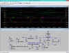
I was able to build out a prototype from the link above and using a simple resistive loads ranging from 330 to 43000 ohms I was able to tune the voltage to about 5volts.
Through this output I connect a usb connector for which I tried to charge an android phone (LG V10). There was indeed charging ongoing, however with the help of a usb doctor which shows the output current, I was only able to get 0.07-0.09 amperes of current.

I have consulted many of my friends and google as well.

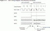
The first solution was that the usb connectors has D- and D+ pins which also provides the exact current for to properly charge a smartphone.
https://electronics.stackexchange.c...ata-pins-d-and-d-on-a-usb-power-adapter-to-be

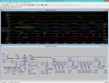
I followed the design of the apple charger (Previously charging an iphone directly doesn't work), and integrate the design to the buck boost converter at the output side as shown below, however I wasn't getting any charge notification at all from the iphone....

upload_2017-11-3_14-38-1.png


The second solution which that the comments suggested a voltage regulator with a higher output current. I tried hooking up with a output of 3A regulator but it didn't work as well.

Is there any solutions for me to make use of the 5V output to charge the smartphone at a current of 1A?

PS:
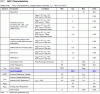
The internal specs given by the buck boost converter was : Input: 6V-30V Output: 0-20V Output Current: 1-2A
 
I can't give advice about the D+ and D- lines since the video covers all I've know about it, but I would like to ask: Have you have tested the power supply with a 5 ohm load? Apparently you only tested it at 15 ma (330 ohms). It may be the power supply that is limiting you to 70 ma or so -better to measure that directly with a meter unless you know the accuracy of USB doctor.

One other question - is you +12V supply holding up? If that sags then the 5V flyback circuit might be running out of margin.
 
Last edited:
I can't give advice about the D+ and D- lines since the video covers all I've know about it, but I would like to ask: Have you have tested the power supply with a 5 ohm load? Apparently you only tested it at 15 ma (330 ohms). It may be the power supply that is limiting you to 70 ma or so -better to measure that directly with a meter unless you know the accuracy of USB doctor.

One other question - is you +12V supply holding up? If that sags then the 5V flyback circuit might be running out of margin.

Thanks for the reply there Mr Cappels.

I can't give advice about the D+ and D- lines since the video covers all I've know about it,
This is ok, I myself don't even know or is even sure if I am correct or not haha. Thus I dare not to modify the D- and D+ again. To which I did tried last 2 weeks ago and the circuit went nuts for which the voltage cannot be adjusted by the trimmer. I then spent close to 5 hours troubleshooting (Bad friday). Only as of today I decided to replace the op amp in the circuit to investigate the issue and found that it was the op amp was not functioning correctly even though there was 5V to the op amp.

Have you have tested the power supply with a 5 ohm load?
For this part, I have tested it with a 10 ohm load on that circuit itself. Anddddddd when I was about the measure the load, I IMMEDIATELY smelled something burning, and I quickly disconnect the load. (Kind of weird...)

to measure that directly with a meter unless you know the accuracy of USB doctor.
The USB Doctor is a china made tester I bought online locally to check for the voltage and current. (**broken link removed** )
I am using a set for testing it onto a anker 5 port charger. It measures about 5.12V and has a output of 1.3-1.4A when I connect to my iphone 6s plus. For which I used that to gauge if my output is working. (The output indeed shows 5.05V on the USB Doctor)
I also measured it with a fluke 87V multimeter at the output, the accuracy is indeed valid. (I am surprised considering the price haha)

One other question - is you +12V supply holding up?
Not sure what you mean by this question. My university's lab is using a bench power supply for which I set it to 12A. ( **broken link removed** )
I only tuned the current a little and the regulators will be active (Turn on).

I would like to apologize for any "no" knowledge of my answers if there's any. Unlike other students who have research graduates who are able to assist them, I am in a situation where this project doesn't have anyone to help me at all. Since I am all alone and stuck, I am deeply appreciative of your help. :)
 
Last edited:
i might be an idiot but i do not see anything that resembles to a buck-boost circuit at that link . . . besides it never specifies it's input nor the output port ???
the inductor value of 330µH is a weird selection for 1A 5W
← is that correct

Thanks for the input ci139!

i do not see anything that resembles to a buck-boost circuit at that link
Erm this is the main circuit of the whole buck boost converter. https://easyeda.com/GreatScott/ATtiny_Buck_Boost_Converter-RXig0YIif
I do not understand why its not a boost even though I was able to tune the voltage all the way to 20V at the output with the help of the trimmer.

the inductor value of 330µH is a weird selection for 1A 5W

I am not a professional and because he gave the internal specs of the circuit which had a output of 1-2A, I thought it would work.... apologies as I have no understanding of this. :(

is that correct
5V and 1A is something is i wish to achieve so yes :) I am unsure of what is your question for this...?
 
thanks for quick reply - i missed the R9 being the "LOAD" -- decoding the schematic . . . ////
VtgBB-QC-10aa.png quick apx. "in operation" -- there seem to be no low power operation limiting figures -- that would show out here ???
it would work
depending on other operational parameters . . . if you consider the ramp up speed at such inductance - it sets the frequency low or the inductor operating near saturation e.g. it requires an inductor that can operate near saturation (having permanent DC component)
5V and 1A is something is i wish to achieve
if the previous quote is what i think it means then the 1A is the minimum load the R9 should have for the thing to work
-------------
 
Last edited:
thanks for quick reply - i missed the R9 being the "LOAD" -- decoding the schematic . . . ////
View attachment 109010 quick apx. "in operation" -- there seem to be no low power operation limiting figures -- that would show out here ???

depending on other operational parameters . . . if you consider the ramp up speed at such inductance - it sets the frequency low or the inductor operating near saturation e.g. it requires an inductor that can operate near saturation (having permanent DC component)

if the previous quote is what i think it means then the 1A is the minimum load the R9 should have for the thing to work
-------------
  • the phone charger may somehow intercept your opamp input
    -- low-pass/integrate your op am input
    -- increase 5V to 5.4V take the output from mosfet side +OUT through schottky add extra caps after that diode
  • the mosfet driver is too weak and/or "goes to a theoretical range" the MOSFET can't follow
    -- requires revising the attiny code for components used
    -- selecting components that can follow the code
    -- using more powerful driver for MOSFET
  • the PCB design introduces noise to MOSFET control chain
    -- sourced from PBC layout itself
    -- +12V AUX SUP and/or +5V AUX SUP and/or the charger as a load


there seem to be no low power operation limiting figures -- that would show out here ???
Thank you so much for simulating the project of mine! However, that was just part of the schematics.
**broken link removed**
This is the full schematic. Apologies for not showing all.

if you consider the ramp up speed at such inductance
May I know how do you go about doing that? I have no clue of what value should i add in?
 
I had to investigate because the connection to your D+ and D- lines looks wrong.
Try removing R1, R10, R11 and R12 and just connecting D+ and D- together (the spec says a short circuit up to a maximum of 200Ω - I suppose it is to allow for different kinds of configuration arrangements). Don't connect them anywhere else. This should give you up to 1.5A charging current - or possibly the maximum the supply can, err, supply.
I believe the standard arrangement with chargers which only supply 500mA (the 1.1 standard) is to connect them together but have a pull up or pull down resistor.
 
if you consider the ramp up speed at such inductance
May I know how do you go about doing that? I have no clue of what value should i add in?
basics - the larger the inductance - the slower the current ramps up on it at MOS-FET switch ON = the inductor's LOAD/UNLOAD SPEED e.g. the speed of the inductor's capability to deliver power -- https://www.schukat.com/schukat/sch...16&refDoc=CMS8C7517EAFA458FEDC1257421002FBF84

your case is not easy to debug as it requires precisely knowing the 'tiny code especially at load step e.g. if you connect the battery - the MCU may interpret it as an overload condition and instead of fast attempting to drive up the output voltage it may go - say - to a power limiting mode . . . from the other hand the lower the inductance the higher the instant power it deliver and the faster switching times (more expensive equipment) are required (here the designer trades in between) . . .
 
Last edited:
t shows 0.03mH on the schematic, so 30uH - makes more sense, yes?
indeed - i assumed a different type of marking at quick glance of photos at instructables - i do have both types the exponent ending and unit ending ones around my place . . .
your correction + schematic + attiny d/s (shows max 20mA sink/source) suggest there might be energy loss at mosfet turn-off or inefficient operating pattern for inductor due "bad" timing control - perhaps ((((i hate to chk it with corrected simulation coz the ±20mA are not the actual port capabilities but ??? allowed max. illustrative values #"¤!!¤&)))) . . . 8ns ?? DS.OFF maybe -- leaves us inductor (not 2+ amp capable) or MPU code (tested for all weather)
 

Attachments

  • VtgBB-QC-10cc.png
    VtgBB-QC-10cc.png
    46 KB · Views: 162
Last edited:
I had to investigate because the connection to your D+ and D- lines looks wrong.
Try removing R1, R10, R11 and R12 and just connecting D+ and D- together (the spec says a short circuit up to a maximum of 200Ω - I suppose it is to allow for different kinds of configuration arrangements). Don't connect them anywhere else. This should give you up to 1.5A charging current - or possibly the maximum the supply can, err, supply.
I believe the standard arrangement with chargers which only supply 500mA (the 1.1 standard) is to connect them together but have a pull up or pull down resistor.

Hi there! Thanks for the response and help throbscottle :)

Try removing R1, R10, R11 and R12 and just connecting D+ and D- together
Sure I will connect the D- and D+ together to see if there is any changes!

upload_2017-11-4_14-0-55.png


It shows 0.03mH on the schematic, so 30uH - makes more sense, yes?
Yes my inductance is about that value, do I need to change the value or something?
 
do I need to change the value or something?
buy a ready made dc/dc converter meeting your i/o powers or build one using dedicated for that an analog switching controller with the d/s recommended parts - as in https://easyeda.com/GreatScott/ATtiny_Buck_Boost_Converter-RXig0YIif the ATTiny does not seem to have any additional data I/O from external computers - then it makes no difference weather you further test someones work or use some other one's finished one

i have been tempted to design a digital psu controller at some times and myself but the options here are that then you have two potential failure sources you need to handle(/error- -service/-proof) -- besides the speedier the required update the more power goes keeping the SPU up to it , e.c. . . . & moreover when in analog control all processes go their schematic defined "natural way" then for numeric control you actually have to code all these "natural ways ..."
 
Last edited:
buy a ready made dc/dc converter meeting your i/o powers or build one using dedicated for that an analog switching controller with the d/s recommended parts - as in https://easyeda.com/GreatScott/ATtiny_Buck_Boost_Converter-RXig0YIif the ATTiny does not seem to have any additional data I/O from external computers - then it makes no difference weather you further test someones work or use some other one's finished one

i have been tempted to design a digital psu controller at some times and myself but the options here are that then you have two potential failure sources you need to handle(/error- -service/-proof) -- besides the speedier the required update the more power goes keeping the SPU up to it , e.c. . . . & moreover when in analog control all processes go their schematic defined "natural way" then for numeric control you actually have to code all these "natural ways ..."

Thanks for the reply ci139

I understand your concern and of course getting a ready made dc-dc converter could have been done way earlier. With that said I would even have finish my project using just a month.
Sadly getting a ready made one isn't much of an option for me as I have to build something from the ground up which was a requirement.
 
Here is the full schematic, something it should *not* have taken 15 posts to achieve:
Schematic-qAsNSH8pW.png

It is not clear where the circuit "output" is. In a non-isolated buck or boost converter, one end of the load usually is tied directly to either Vcc or GND. Also, there is no buck here; this circuit can only boost.

ak

Hi there Ak, thanks for the reply!

The output is at R9 which is the load section.
I was able to buck and boost in terms of the voltages. However I was not able to get a decent output current.


I have several questions that I was wondering if anyone could answer:
1)The attiny85 he used, is that to produce a square wave to control the mosfet?
2)Why is there a need for the op amp in the circuit?
 
how to use the blow documents
  • in case your time budget is limited
    • fast filter out the parts or sentences that relate/apply(somewhat) to your case -- use them as approximate rulers or guiding margins for what there could be or should be also in your design
    • try to get the cause/reason and the result/effect of the presented wave forms in a circuit they apply to - compare with your circuit - as for what to adjust (for your circuit to work) or remake (for your circuit to work better as it currenlty is set/designed to - if you are sure/convinced has such an effect)
  • in case your schedule is more flexible
    • read and try to systematize the presented knowledge (for further purposes -- even such as from where to find from if required : bookmark or a local copy of entire doc or a copy of the appended document references)
    • ??? test some simple example circuits or parts of them on pin board to increase your self assurance and get some practical experience such as your cmos - over the top input - level shifter - op amp sub circuit
      Test-Test.gif
    something i forgot -- your mathematics (← a random link to) , eletrostatics , electrodynamics must be good or at least sufficient -- if it's not -- set up a progress plan or ask someone to assist you with (start from simple tasks that you are interested in , move forward when you get more familiar with what the next topics will be and you start getting an idea of how to deal with)
Buck Converter Selection Criteria https://www.richtek.com/my/Design Support/Technical Document/AN033
Design Calculations for Buck-Boost Converters **broken link removed**
Design tips for an efficient non-inverting buck-boost converter https://www.ti.com/lit/an/slyt584/slyt584.pdf
Investigation on Interleaved Boost Converters and Applications , Chuanyun Wang https://citeseerx.ist.psu.edu/viewdoc/download?doi=10.1.1.462.1090&rep=rep1&type=pdf
LM2596 SIMPLE SWITCHER® Power Converter 150-kHz 3-A Step-Down Voltage Regulator https://www.ti.com/lit/ds/symlink/lm2596.pdf
TPS6306x High Input Voltage, Buck-Boost Converter With 2-A Switch Current https://www.ti.com/lit/ds/symlink/tps63060.pdf
A5974AD Up to 2 A step-down switching regulator for automotive applications https://www.st.com/content/ccc/reso...df/jcr:content/translations/en.DM00027259.pdf

2)Why is there a need for the op amp in the circuit?
?? what is the voltage range at V(D1,C4) and V(L1,C4) and vhat is the voltage range U3.Pin-1 or U2.Pin-2
 
Last edited:
Design of a DC/DC buck converter for ultra-low power applications in 65nm CMOS Process -- with component selection and misc. feedback filters' examples e.g. what to do with your c-mos op-amp
=======
img. -- a dummy filter test -- since your specific setup has "highly variable" input (relative to c-mos supply) ↑the above↑ much likely can't be adapted without compensating against this
____ while the example just illustrates a difference of RAW and smoothed output (PS! the simulation is illustrative and uses a different component values than those in your circuit -- among other causes is i've not yet bothered to explore the attiny operation !!!)
 

Attachments

  • VtgBB-QC-10dd.png
    VtgBB-QC-10dd.png
    52.3 KB · Views: 168
Last edited:
i expexted 100x more of (several kb-s of) the MCU code ??
about https://www.instructables.com/id/DIY-BuckBoost-Converter-Flyback/ :: https://cdn.instructables.com/ORIG/FZE/1LU4/IU2NFBF2/FZE1LU4IU2NFBF2.ino
Code:
#define F_CPU 8000000
const int pwm = 1;
const int potinput = A1;
const int feedbackinput = A3;
int potinputval;
int feedbackinputval;
int pwmval;

void setup() {
  TCCR0A = 2 << COM0A0 | 2 << COM0B0 | 3 << WGM00;
  TCCR0B = 0 << WGM02 | 1 << CS00;
  TCCR1 = 0 << PWM1A | 0 << COM1A0 | 1 << CS10;
  GTCCR = 1 << PWM1B | 2 << COM1B0;
  pinMode(pwm, OUTPUT);
  pinMode(potinput, INPUT);
  pinMode(feedbackinput, INPUT);
  digitalWrite(pwm, LOW);
  pwmval = 0;
}

void loop() {
  potinputval = analogRead(potinput);
  feedbackinputval = analogRead(feedbackinput);
  while (feedbackinputval < potinputval){
   if (pwmval > 203){
     analogWrite(pwm, pwmval);
     potinputval = analogRead(potinput);
     feedbackinputval = analogRead(feedbackinput);
   }
   else {
   analogWrite(pwm, pwmval);
   pwmval = pwmval + 1;
   potinputval = analogRead(potinput);
   feedbackinputval = analogRead(feedbackinput);
  }}
  while (feedbackinputval > potinputval){
   if (pwmval == 0){
     analogWrite(pwm, pwmval);
     potinputval = analogRead(potinput);
     feedbackinputval = analogRead(feedbackinput);
   }
   else{
   analogWrite(pwm, pwmval);
   pwmval = pwmval - 1;
   potinputval = analogRead(potinput);
   feedbackinputval = analogRead(feedbackinput);
   }}
}
all it takes now is to find some virtual tiny or many weeks of reading the spec.-s
it seems the 1MHz input rate can be configured but is not recommended (related)
which means that you might need to use an inductor with multiples of higher inductance to achieve 1.5A output current
it seems the 38.4kHz comes from Max. recommended 1MHz ADC Clk / 13 e.g. a 76.9ksps input rate resulting in incoming signal bandwith of 38.5kHz
 

Attachments

  • Fig-17-07.gif
    Fig-17-07.gif
    9.6 KB · Views: 148
  • Fig-21-07.gif
    Fig-21-07.gif
    29.8 KB · Views: 175
Last edited:
Status
Not open for further replies.

Latest threads

New Articles From Microcontroller Tips

Back
Top