Continue to Site

Welcome to our site!

Electro Tech is an online community (with over 170,000 members) who enjoy talking about and building electronic circuits, projects and gadgets. To participate you need to register. Registration is free. Click here to register now.

  • Welcome to our site! Electro Tech is an online community (with over 170,000 members) who enjoy talking about and building electronic circuits, projects and gadgets. To participate you need to register. Registration is free. Click here to register now.

Current Regulator w/ FET, NPN transistors

Status
Not open for further replies.

stryker1080

New Member
Hi everyone, I am a mechanical engineer who is in need of help! I am designing an underwater flashlight which will be using Luxeon high power leds. I have found a driver circuit which uses FET and NPN transistors and i was hoping someone can help me disect it a bit.

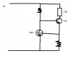
I have done a bit of research so i have a basic understanding of how NPN and FET transistors work, but i was hoping someone can just clarify a few things. I have attached the circuit drawing.

Basically at the end of the day, i want to limit the current going through the LEDs to 1A. My understanding of how this circuit is supposed to work is this:

- The bottom right resistor is chosen so that when maximum wanted current is going through it, the voltage drop is equal to the "turning on" voltage of the NPN (ie. ~.5V) . So I need a I=V/R => 1 = 0.5/R = > R = 0.5 Ohm
- When the circuit draws too much current, the NPN transistor opens up and the current goes mainly through the NPN transistor instead of the FET and it limits the current? THe reason i have trouble understanding this is because i read that FET transistors are voltage regulated, and in order to minimize the curretn going through the FET a -ve voltage is needed?
- How do you calculate the voltage drop going through a transistor? Is there any voltage drop?
- How do you select the resistance of the Top Left resistor?
- When the NPN transitor opens up, wont all the current go though it instead of the FET and completely shut off current going through the Load? How would this work as a self-adjusting circuit?

Hopefully someone can describe in detail what is going on with this type of circuit, i apologize for my lack of knowledge. I have been searching and reading the forums to piece together knowledge to find out how this is supposed to work.

Thanks!
 

Attachments

  • circuit.jpg
    circuit.jpg
    11.4 KB · Views: 334
hi,
The FET and resistor R2 to 0V, together with the voltage on the gate of the FET form a Constant Current source.

The value of the current flowing thru the FETand LED is determined by the value of the resistor R2 and the voltage on the gate of the FET, which is determined by the collector voltage on the transistor.

So when the current flowing thru R2 causes a voltage drop across R2 equal to the +0.7v required to switch on the transistor, it conducts and the voltage on the gate of the FET falls, this reduces the current in the FET and the LED.

So the current flowing in the FET/LED is limited.

What type of FET are you using.

The voltage on the FET gate is controlled by the value of R1 and the gate operating voltage of the FET. Refer to the FET's datasheet.

Does this help.?
 
Last edited:
But what is preventing all the current from being sucked through the NPN when it is turned on and as a result not providing enought voltage to the FET thereby shutting off the LEDs completely? When the NPN is turned on, can you not consider the collector-emmiter line to be like a straight wire with no resistance?

Do you think you could possibly go though calculations for that circuit to determine what R1, R2 and FET/NPN transistors i need to draw 1A of current to the leds? That way i would be able to go through the design process and how you are supposed to calculate these. My problem is that i am not sure what depends on what. Like the FET will give a certain current based on base voltage regardless of the emmiter-collectro voltage drop? Im also confused on how if the e-c voltage drop is less than 2 (or close to the base voltage) then the current is controled by the voltage of the e-c, and if the e-c voltage is more than the gate voltage controls it?
 
So far for the calculations i have this:

R2 needed: V=IR -> 0.5 = 1A*R2 -> R2=.5 ohm
Vdrop FET (using 6V power supply, 1 LED which draws 3.7V @ 1A) :
Vfet = 6 - 3.7 - .5 (NPN activation) = 1.8V

Now i am kinda stuck on how to get the base voltage of FET or the R1 i need...
 
stryker1080 said:
But what is preventing all the current from being sucked through the NPN when it is turned on and as a result not providing enought voltage to the FET thereby shutting off the LEDs completely?
Because the NPN will NOT turn ON until the current flowing in the R2/FET/LED reaches a value that creates a voltage drop across R1 equal to +0.7V,

When the NPN is turned on, can you not consider the collector-emmiter line to be like a straight wire with no resistance?
NO, It has a an 'apparent' resistance

Do you think you could possibly go though calculations for that circuit to determine what R1, R2 and FET/NPN transistors i need to draw 1A of current to the leds?
If you want a FET/LED current of about 1amp, then the R2 value would be 0.7ohms.. [ Volts= amps * resistance] V= 1 * 0.7R = 0.7V, which turns on the transistor.

That way i would be able to go through the design process and how you are supposed to calculate these. My problem is that i am not sure what depends on what. Like the FET will give a certain current based on base voltage regardless of the emmiter-collectro voltage drop? Im also confused on how if the e-c voltage drop is less than 2 (or close to the base voltage) then the current is controled by the voltage of the e-c, and if the e-c voltage is more than the gate voltage controls it?

hi,
The FET is a gate voltage controlled device, within the limits of the FET design, for the FET shown in your drawing, the higher the gate voltage the more current it passes. Until the R2 voltage drop switches on the NPN and the gate voltage is pulled down by the NPN thus reducing the FET current.

If you want to check out a circuit without blowing an LED, then in place of the LED connect a current meter able to indicate say 3 amps and the adjust the value of R2 until 1Amp flows in the meter.

The value of R1 would be around 10K

Is this clear.?
 
But what is preventing all the current from being sucked through the NPN when it is turned on and as a result not providing enought voltage to the FET thereby shutting off the LEDs completely?
Because the NPN will NOT turn ON until the current flowing in the R2/FET/LED reaches a value that creates a voltage drop across R1 equal to +0.7V,

Ok this makes sense, but how can you tell what the actual final current in that branch will be? Sure the NPN can turn on and redirect the current, but what if it doesnt redirect enough and the current ends up stabilizing at 1.5 A? All that NPN does is ensure the switch turns on at 1A, but whats preventing from the current from overshooting.

hi,
The FET is a gate voltage controlled device, within the limits of the FET design, for the FET shown in your drawing, the higher the gate voltage the more current it passes. Until the R2 voltage drop switches on the NPN and the gate voltage is pulled down by the NPN thus reducing the FET current.

If you want to check out a circuit without blowing an LED, then in place of the LED connect a current meter able to indicate say 3 amps and the adjust the value of R2 until 1Amp flows in the meter.

The value of R1 would be around 10K

Is this clear.?

There is another question i had, from other Electronic design sources, i read that in order to reduce the current that runs through the collector-emmiter you need to apply a -ve voltage. How can you possibly get a -ve voltage at the base with the circuit that you posted?

The value of R1 would be around 10K

Could you explain how you got this number? How did you calculate the current/voltage through that resistor?

I really appreciate your help, i hope you dont mind my constant questions... Unfortunately i have a hard time of letting things go which i do not understand fully...
 
stryker1080 said:
Ok this makes sense, but how can you tell what the actual final current in that branch will be? Sure the NPN can turn on and redirect the current, but what if it doesnt redirect enough and the current ends up stabilizing at 1.5 A? All that NPN does is ensure the switch turns on at 1A, but whats preventing from the current from overshooting.
The current will settle at a value of about 0.7V across R2 since that is the voltage needed to turn on the NPN transistor. Thus the current is ~0.7V/R2. If the current varies from this the NPN will either conduct more or less which adjusts the current through the FET to bring everything back into balance. It's the miracle of negative feedback.

stryker1080 said:
There is another question i had, from other Electronic design sources, i read that in order to reduce the current that runs through the collector-emmiter you need to apply a -ve voltage. How can you possibly get a -ve voltage at the base with the circuit that you posted?
I'm not sure what this source is talking about. To reduce the collector current you simply reduce the base current (Which slightly reduces the base-emitter voltage. The base emitter junction looks like a diode.)

Remember that bipolar transistors are basically current controlled and FETS are voltage controlled. Both devices act rather like current sources, that is their collector/drain currents are relatively independent of the collector/drain voltage. It only depends upon the base current or gate voltage respectively.
 
Ok, i have some updates:

I went back to the site which had the circuit on how to construct this current limiter and they were using a Fairchild FQP50N06L FET transistor. I looked up the specs of it and it is a MOSFET N-channel Enhanchement mode. I looked up what this means, and this particular type of FET is ALWAYS OFF unless a small POSITIVE voltage to the base is applied. Now this is starting to make sense how the NPN will actually limit.

Ok so i think i have a decent understanding of how the negative feedback works usiing these transistors. The only thing i still want to know is what is the purpose of R1? My guess would be that it is there to limit the current that will be going into the FET so to not "blow" it up? How would you go about calculating the value of resistor you need?
 
stryker1080 said:
Ok, i have some updates:

I went back to the site which had the circuit on how to construct this current limiter and they were using a Fairchild FQP50N06L FET transistor. I looked up the specs of it and it is a MOSFET N-channel Enhanchement mode. I looked up what this means, and this particular type of FET is ALWAYS OFF unless a small POSITIVE voltage to the base is applied. Now this is starting to make sense how the NPN will actually limit.

Ok so i think i have a decent understanding of how the negative feedback works usiing these transistors. The only thing i still want to know is what is the purpose of R1? My guess would be that it is there to limit the current that will be going into the FET so to not "blow" it up? How would you go about calculating the value of resistor you need?
hi,
Pleased that you follow the voltage control of the FET gate.

The purpose of R1 is to control the voltage on the FET gate.

Consider that the NPN is NOT conducting, then the full supply voltage would be applied to the FET gate via the R1 resistor.

This would make the FET conduct as its a positive voltage, as the FET conducts the voltage drop across R2 will rise to about +0.7V which will turn ON the NPN transistor, so current will flow in R1 and the voltage at the NPN collector/FET gate will fall. This fall will reduce the current in the FET.

At some point a balance will be reached between the voltage drop in R2 and the conduction of the NPN. [ in other words the gate voltage on the FET].

At balance, due to negative feedback the current in the FET will be constant.

R1 is not there to limit the current into the FET gate, the FET gate draws almost zero current. Its a Field Effect Transistor, the gate voltage creates an electric field inside the FET, which controls the amount of current flowing from Source to Drain in the FET.
The value of R1 is chosen to suit the gain required by the NPN, I have chosen 10K as a starting point.

Whats the battery voltage going to be.??

Does this help.:)
 
hi,
Redrawn the circuit, added some values.

Is this clearer.?:rolleyes:
 
Last edited:
Ok, this is starting to make more sense but has also raised a few more questions (bear with me...).

Consider that the NPN is NOT conducting, then the full supply voltage would be applied to the FET gate via the R1 resistor

If the NPN is not conducting, how would the full supply voltage be applied to the FET gate? If there is almost no current going through the FET through the base, how would you do a voltage drop loop in this circuit? Would it be Vsupply - VR1 - (Vfet Base-Emmiter) - VR2 = 0? Was R1 selected to give a voltage drop corresponding to the max output current for the FET?

The value of R1 is chosen to suit the gain required by the NPN, I have chosen 10K as a starting point.

What do you mean chosen to suit the gain?

Whats the battery voltage going to be.??
Well the battery voltage is going to be variable. I wanted this circuit to be able to drive 1, 2 or 3 or however many LEDs i want. The brief instructions on how to set it up mentioned that it can work with as many LEDs as you want as long as the voltage source is higher than LEDs draw + ~.5 V for dropout voltage (guessing this is the NPN). The author wrote that if you select a voltage source that is higher than required by the LEDs, then the FET will just disipate this extra energy as heat and with a proper heatsink it would be ok.
 
stryker1080 said:
Ok, this is starting to make more sense but has also raised a few more questions (bear with me...).


If the NPN is not conducting, how would the full supply voltage be applied to the FET gate? If there is almost no current going through the FET through the base, how would you do a voltage drop loop in this circuit?

When the NPN is NOT conducting its open circuit, so no current flows thru collector resistor, therfore there is NO voltage drop across the R1 resistor, so the full battery voltage is applied to the FET gate. The FET switches very quickly and it starts tp pass current in the LED circuit and R2. The voltage drop across R2 [0.6V] starts the NPN conducting and that causes current to flow in the collector resistor pulling the gate voltage down.

Remember the FET gate draws NO current.

What do you mean chosen to suit the gain?
I have chosen a NPN current of 1mA, which according to the datasheet gives a gain of about 50.

Well the battery voltage is going to be variable. I wanted this circuit to be able to drive 1, 2 or 3 or however many LEDs i want. The brief instructions on how to set it up mentioned that it can work with as many LEDs as you want as long as the voltage source is higher than LEDs draw + ~.5 V for dropout voltage (guessing this is the NPN). The author wrote that if you select a voltage source that is higher than required by the LEDs, then the FET will just disipate this extra energy as heat and with a proper heatsink it would be ok.

Refer the last pdf drawing.
Does this answer you questions.?

The voltage drops across the resistors are determined by using Ohms law.
 
I don't mean to confuse the issue but if you're interested in maximum battery life than a switching regulator configured to generate a constant current can be used. This has higher efficiency than a series regulator, particularly if the battery voltage is significantly higher than the sum of the LED voltages. If you're interested in such an approach an example of this is discussed at **broken link removed**.
 
If the NPN is not conducting, how would the full supply voltage be applied to the FET gate? If there is almost no current going through the FET through the base, how would you do a voltage drop loop in this circuit?

When the NPN is NOT conducting its open circuit, so no current flows thru collector resistor, therfore there is NO voltage drop across the R1 resistor, so the full battery voltage is applied to the FET gate. The FET switches very quickly and it starts tp pass current in the LED circuit and R2. The voltage drop across R2 [0.6V] starts the NPN conducting and that causes current to flow in the collector resistor pulling the gate voltage down.

Ok, that makes total sense now. Thank you.

What do you mean chosen to suit the gain?
I have chosen a NPN current of 1mA, which according to the datasheet gives a gain of about 50.

So just to clarify, you have selected to send 1ma to the BASE which turns on. This NPN has a gain of 50 so the current going through the collector-emmiter will be 50ma. Is that correct? If it is, i have several questions stemming from this:

- How do you know that 1ma will be going to the base? All we know is that the voltage drop from base-emmiter will be 0.7V and 1A goes through R2.
- If we know that 50ma is going through R1, we can calculate what the voltage drop would be and consequently what the new BASE FET voltage is correct? and we know what voltage we need to give a certain current from the FET collector-emmiter, and this way we can find R1 right?


Also, one other thing that just popped in my head. I looked at the specs for the MOSFET, and if a 6+ volt is applied , the emmiter-collector current is 100 A?! If i had 3 leds and i need about 12V to supply them, and i need 1A (needs a 2V gate), where would the leftover 10V go??
 
crutschow said:
I don't mean to confuse the issue but if you're interested in maximum battery life than a switching regulator configured to generate a constant current can be used. This has higher efficiency than a series regulator, particularly if the battery voltage is significantly higher than the sum of the LED voltages. If you're interested in such an approach an example of this is discussed at **broken link removed**.

I will look into this as well, thank you!
 
A dedicated switching IC for driving up to 5 LEDs is the Texas Instruments TPS61060/61/62 series of devices.
 
hi stryker,

So just to clarify, you have selected to send 1ma to the BASE which turns on. This NPN has a gain of 50 so the current going through the collector-emmiter will be 50ma. Is that correct? If it is, i have several questions stemming from this:
Its not the base current I have set at 1mA, its the collector current

- How do you know that 1ma will be going to the base? All we know is that the voltage drop from base-emmiter will be 0.7V and 1A goes through R2.
- If we know that 50ma is going through R1, we can calculate what the voltage drop would be and consequently what the new BASE FET voltage is correct? and we know what voltage we need to give a certain current from the FET collector-emmiter, and this way we can find R1 right?
There never could be 50mA flowing thru R1, use ohms law.

Also, one other thing that just popped in my head. I looked at the specs for the MOSFET, and if a 6+ volt is applied , the emmiter-collector current is 100 A?! If i had 3 leds and i need about 12V to supply them, and i need 1A (needs a 2V gate), where would the leftover 10V go??
The FET current can never get higher than 1Amp with the values shown.
Lookup negative feedback, from the NPN, the current in the FET is a Constant Current of 1Amp.


The voltage difference between the supply and the voltage drop across the LEDs [in SERIES] would be across the FET.

In a case like that the 10V at 1amp [considering just one LED] would generate a heating effect of 10Watts, you would need a heat sink on the FET.

You must NOT connect the LED's in parallel.

Are we there yet..:rolleyes:
 
So just to clarify, you have selected to send 1ma to the BASE which turns on. This NPN has a gain of 50 so the current going through the collector-emmiter will be 50ma. Is that correct? If it is, i have several questions stemming from this:
Its not the base current I have set at 1mA, its the collector current

So you selected the 1ma based on the BASE EMMITER ON voltage VS collector chart on the NPN specs sheet? Basically you can get the collector current based off the on voltage to the base... On the NPN i am looking at i would have about 10mA of current with the 0.7V base voltage.

Also, one other thing that just popped in my head. I looked at the specs for the MOSFET, and if a 6+ volt is applied , the emmiter-collector current is 100 A?! If i had 3 leds and i need about 12V to supply them, and i need 1A (needs a 2V gate), where would the leftover 10V go??
The FET current can never get higher than 1Amp with the values shown.
Lookup negative feedback, from the NPN, the current in the FET is a Constant Current of 1Amp.

Yes that makes sense, without the NPN negative feedback there the current would go to 100A, but as soon as it rises to 1A, the NPN turns on and brings the current to stabilize...


And to select R1. I look at the specs of the MOSFET such as the FQP50N06L. To get 1A drain current, the gate voltage must be ~2.4V . Knowing this, we want to select R1 to give that voltage to the FET. Using a power supply of 6V, we need a 6-2.4V = 3.6V drop. So R= V/I = 3.6/10mA = 360 ohm?

Am i getting it haha? I think im starting to understand it better lol.
 
stryker1080 said:
So you selected the 1ma based on the BASE EMMITER ON voltage VS collector chart on the NPN specs sheet? Basically you can get the collector current based off the on voltage to the base... On the NPN i am looking at i would have about 10mA of current with the 0.7V base voltage.

To elaborate on my previous comments about bipolar transistors: The base-emitter voltage is always around 0.6-0.7V (typical of a foward biased diode) when the transistor is on. It's the base current that determines the collector current. The base voltage will vary slight with base current of course (again similar to a diode) but it's the current that is the determining factor.

If you look at the gain curves for a transistor it will typically peak over some collector current range and droop at the high and low current levels. Typically you want to bias the transistor so its collector current is somewhere in the peak range of gain, in this case 1mA was selected.

In your calculation for R1 you used 10mA, it should be 1mA. Also the 2.4V gate voltage is actually gate-to-source voltage. Thus you need to add the 0.7V source voltage (across R2) to the 2.4V gate-source voltage to give 3.1V required at the gate (to common). Thus R1 = (6V-3.1V) / 1mA = 2.9k ohm.
 
Status
Not open for further replies.

Latest threads

New Articles From Microcontroller Tips

Back
Top